Structure and method for enhancing resistance to fracture of bonding pads

a technology of bonding pads and structures, applied in the direction of semiconductor devices, semiconductor/solid-state device details, electrical apparatus, etc., can solve the problems of lack of bonding pad area for wiring purposes, failure of electric bonding pads, slow degradation and reliability problems, etc., to facilitate the cmp process, improve the flexibility of wiring, and enhance the flexibility of metal wiring

Inactive Publication Date: 2008-05-15
MARVELL ASIA PTE LTD
View PDF26 Cites 17 Cited by
  • Summary
  • Abstract
  • Description
  • Claims
  • Application Information

AI Technical Summary

Benefits of technology

[0021]Not only does the bottom surface of the bond pad itself adhere to the insulating layer immediately below in this structure, but the walls of the multiple first metal vias and surfaces of all the vertical alternating stacks not adjoining the multiple first metal vias also adhere to the dielectrics surrounding them. The area of adhesion between the dielectric material in the back end of the line film stack and the contiguous and conducting extension of the bond pad, including the bond pad itself and the multiple vertical alternating stacks, is increased significantly.
[0022]A portion of pad area within the metal level below the bond pad, wherein the multiple metal pads are located, may be utilized to electrically connect the bond pad to the integrated circuit elements on the chip and to provide enhanced flexibility in metal wiring in this structure. Also, the unused portion of the pad area within the metal level below the bond pad may also utilized for a second set of metal wires for passing current from another part of the semiconductor chip through the pad area within the metal level below the bond pad to yet another part of the semiconductor chip. If some unused area still remains in the pad area within the metal level below the bond pad, metal fills may optionally be used to facilitate the CMP process.
[0023]The adhesion between the bond structures according to the various aspects of the present invention is superior to prior art structures without any via below a bond pad while the flexibility of wiring is better than prior art structures wherein the bond pad structure occupies multiple levels of metal layers.

Problems solved by technology

These may cause cracks in the bonding structure causing electrical failure of the bonding pad or slow degradation and reliability problems due to ingress of ambient atmosphere, especially moisture into the chip.
One disadvantage of this approach is the lack of availability of the bonding pad area for wiring purposes.
Thus, metal wiring is severely limited under the bond pad.
While the structure above provides maximum flexibility for wiring, the mechanical strength of the structure is not sufficient to provide a reliable structure under stress.

Method used


Image

  • Structure and method for enhancing resistance to fracture of bonding pads
  • Structure and method for enhancing resistance to fracture of bonding pads
  • Structure and method for enhancing resistance to fracture of bonding pads

Examples


first embodiment

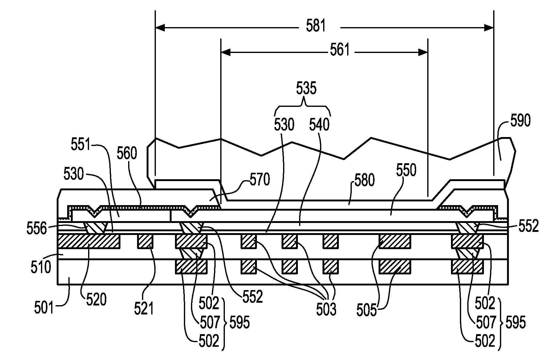
[0048]According to the present invention, a first bond pad structure 500 is described in FIGS. 5-6. FIG. 5 is a schematic top-down view, while FIG. 6 is a schematic cross-sectional view along the line B-B′ in FIG. 5. The first bond pad structure 500 has a first metal pad 550, which is a bond pad, in the first layer of the structure. The area inside the periphery of the first metal pad 550 is referred to as the “pad area.” Only one contiguous first metal pad is necessary for the formation of one of the first bond pad structure 500. The first metal pad 550 is made of metal, and preferably a stack of a liner material and an aluminum alloy. A bond pad extension 551, adjoining the bond pad 550, built on the same level as a bond pad 550, and consisting of the same material as the bond pad, may optionally be constructed as well. The liner material may comprise a stack of tantalum nitride (TaN), titanium (Ti), and titanium nitride (TiN) or an alternate stack of metals with good adhesion pro...

second embodiment

[0063]According to the present invention, the center area 558 of the bond pad structure 700 does not contain any second metal pad 522. All the metal pads are confined within the peripheral area 559. All of the first metal vias 552 are also located within the peripheral area 559. Furthermore, at least one metal structure that does not contact any of the first metal vias 552 is placed within the pad area and at the same level as the second metal pads 522. The metal structure can be either first metal fills 523 or at least one first metal wire 525. None of the first metal fills 523 or any of a portion of the first metal wires 525 is adjoined by any of the first metal vias 552. In other words, there are no metal vias within the pad area that connect any of the metal fills 23 or any of a portion of the first metal wires 525 to the first metal pad 550 above.

[0064]Any of the first metal wires 525 may extend outside the pad area to make electrical connections to other components of the inte...

seventh embodiment

[0074]the present invention enables the use of the pad area at the same level as the second metal pads for wiring the bond pad 550 to the integrated circuit elements below. Alternatively, the second metal wires 524 may be used with existing wiring scheme to reduce the resistance of the circuit wiring path from the bond pad 550.

[0075]According to an eighth embodiment of the present invention, an eighth bond pad structure 1500 is described in a schematic top-down view in FIG. 15. The eighth bond pad structure 1500 according to the present invention shares all the elements of the seventh bond pad structure 1300 according to the seventh embodiment. Furthermore, at least one metal structure that does not contact any of the first metal vias 552 is placed within the pad area and at the same level as the second metal pads 522. The metal structure can be either first metal fills 523 or at least one first metal wire 525. None of the first metal fills 523, nor any of a portion of the first met...


PUM


Abstract

The present invention provides bond pads structures between semiconductor integrated circuits and the chip package with enhanced resistance to fracture and improved reliability. Mismatch in the coefficient of temperature expansion (CTE) among the materials used in bond structures induces stress and shear on them that may result in fractures within the back end dielectric stacks and cause reliability problems of the packaging. By placing multiple metal pads which are connected to the bond pad through multiple metal via, the adhesion between the bond pads and the back end dielectric stacks is enhanced.

Description

FIELD OF THE INVENTION[0001]The present invention relates to semiconductor structures, and particularly, to bonding pad structures.BACKGROUND OF THE INVENTION[0002]In the semiconductor industry, a bond pad refers to a contiguous metal pad typically formed out of the last layers of metal during a semiconductor manufacturing sequence. A bond pad is typically large enough to accommodate the bottom portion of a solder ball. A bond pad structure refers to a structure containing such a bond pad and surrounding or attached structure, which as a whole helps accommodate the solder ball.[0003]Once the fabrication of integrated circuit elements on a semiconductor substrate is completed, the semiconductor substrate is diced and packaged in a bonding process. Bond pads provide a structure for electrical connection between the fabricated integrated circuit elements and the package. Typically, one end of an interconnection wire is bonded to a bond pad and the other end is bonded to the next level ...

Claims


Application Information

Patent Timeline
Patent Type & Authority Applications(United States)
IPC IPC(8): H01L23/52H01L21/768
CPCH01L24/05H01L2224/0401H01L2924/0002H01L2924/01033H01L2924/01019H01L2924/01006H01L2924/00013H01L2224/131H01L2224/02235H01L24/13H01L2224/05094H01L2224/02351H01L2224/05095H01L2924/14H01L2924/05042H01L2924/04953H01L2924/04941H01L2924/014H01L2924/01082H01L2224/05073H01L2224/05572H01L2224/05624H01L2224/05647H01L2224/13006H01L2224/16H01L2924/01005H01L2924/01013H01L2924/01014H01L2924/01022H01L2924/01029H01L2924/0105H01L2924/01057H01L2924/01073H01L2924/00014H01L2224/05599H01L2224/13099H01L2224/05099H01L2224/13599H01L2224/29099H01L2224/29599H01L2224/05552
Inventor MELVILLE, IAN D.FAROOQ, MUKTA G.JUNG, DAE YOUNG
Owner MARVELL ASIA PTE LTD
Why Eureka
Try Eureka