Ultraviolet light-emitting element, ultraviolet light-emitting element packaging body and manufacturing method thereof

A technology of light-emitting components and packages, which is applied in the direction of electrical components, semiconductor devices, circuits, etc., can solve problems such as reflow soldering bubbles, cutting off, vibration off, etc., to prevent easy cracking, increase light output efficiency, increase adhesion or adhesion sexual effect

Active Publication Date: 2019-10-22
XIAMEN SANAN OPTOELECTRONICS CO LTD
View PDF5 Cites 6 Cited by
  • Summary
  • Abstract
  • Description
  • Claims
  • Application Information

AI Technical Summary

Problems solved by technology

But it is difficult to process, and it is prone to problems such as cutting off, vibration off, reflow soldering bubbles, etc.

Method used


Image

  • Ultraviolet light-emitting element, ultraviolet light-emitting element packaging body and manufacturing method thereof
  • Ultraviolet light-emitting element, ultraviolet light-emitting element packaging body and manufacturing method thereof
  • Ultraviolet light-emitting element, ultraviolet light-emitting element packaging body and manufacturing method thereof

Examples


Embodiment 1

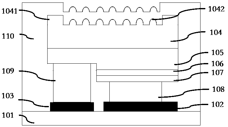
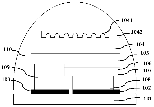
[0049] The invention provides a package body of an ultraviolet semiconductor light-emitting element, which belongs to the technical field of LED light-emitting. Such as figure 1 As shown, the package includes a substrate 101 on which a flip-chip ultraviolet semiconductor light-emitting element is mounted.

[0050] In this embodiment, the substrate 101 is formed of any material. For example, metals, ceramics, resins, dielectrics, pulp, glass, paper, composites thereof, or composites of these materials and conductive materials (eg, metals, carbon, etc.) may be mentioned. Metals include metals containing copper, iron, nickel, chromium, aluminum, silver, gold, titanium or alloys thereof. Examples of resins include epoxy resins, bismaleimide triazine (BT) resins, polyimide resins, and the like. The resin may contain white pigments such as titanium oxide. Among them, ceramics are preferable.

[0051] Examples of ceramics include those containing aluminum oxide, aluminum nitrid...

Embodiment 2

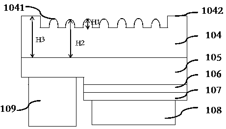
[0095] As an alternative to Embodiment 1, this embodiment provides Figure 10 In the schematic diagram of the structure of the ultraviolet semiconductor light-emitting element shown, the second surface side of the light-transmitting substrate 104 includes a first region 1041, and the height of the uneven pattern on the surface of the first region is H4, and the range of H4 is 0.1-2 μm. The thickness from the rough pattern surface to the first surface side of the substrate is H5, the thickness of H5 is more than 250 μm, the second surface side includes a second region 1042, and the surface of the second region 1042 is Relatively flat, relatively flat may be absolutely flat or the height of the uneven topography is less than 5nm. The thickness H6 from the surface of the second region 1042 on the second surface side to the first surface side is H6, the thickness H6 of the second region 1042 is lower than H5 of the first region 1041, and the difference between H5 and H4 is larger ...


PUM


Abstract

An ultraviolet semiconductor light-emitting element includes: a light-transmitting substrate, a semiconductor layer, and an electrode with opposite electrical properties, wherein the semiconductor layer and the electrode with opposite electrical properties are positioned on the first surface side of the light-transmitting substrate. The ultraviolet semiconductor light-emitting element is characterized in that the light-transmitting substrate is provided with a second surface side which is laterally opposite to the first surface and is a light-emitting surface side; the second surface side is divided into a first area on the inner side and a second area on the outer periphery; the first region is patterned or coarsened to be uneven; the second area is a relatively flat area relative to thefirst area; and the thickness of the substrate of the first area is smaller than that of the substrate of the second area or the thickness from the bottom of the uneven morphology of the first area tothe first surface side of the substrate is equal to or larger than the thickness of the substrate of the second area. Through the uneven morphology of the first area, the adhesion of the packaging resin is effectively improved; the second area effectively prevents the resin from being damaged and achieves a buckling effect on the packaging resin; and the light emitting effect is improved.

Description

technical field [0001] The invention relates to a packaging body, which is especially suitable for the packaging of ultraviolet LED chips. Background technique [0002] Ultraviolet LED chips (λ≤340nm), as a light source with the advantages of high efficiency, energy saving, and portability, can be used in the fields of air and water purification, medical sterilization, and disinfection UV curing. Because the ultraviolet light source has obvious cracking and yellowing problems for many organic materials. In particular, the photons in the ultraviolet band will cause the silicone material commonly used in LED light-emitting diode packaging devices to crack. In order to avoid the degradation of device stability caused by the cracking of the protective colloid of the package, people use glass and other inorganic materials instead of the package glue, but the combination of the substrate and the glass material is difficult to achieve, and the cost of inorganic materials with good...

Claims


Application Information

Patent Timeline
Patent Type & Authority Applications(China)
IPC IPC(8): H01L33/20H01L33/22H01L33/54
CPCH01L33/20H01L33/22H01L33/54
Inventor 臧雅姝李水清江宾林素慧蔡伟龙彭康伟
Owner XIAMEN SANAN OPTOELECTRONICS CO LTD
Why Eureka
Try Eureka