This helps you quickly interpret patents by identifying the three key elements:
Problems solved by technology
Method used
Benefits of technology
Benefits of technology
[0010]Accordingly, the present invention has been made keeping in mind the above problems occurring in the prior art, and an aspect of the present invention is to provide an optical switch, which has advantages of an MEMS optical switch and a waveguide optical switch including lower electric power consumption, an easier packaging process, and a faster switching speed.
[0013]The optical switch according to the present invention has a structure in which the moving waveguides move by the actuator with the MEMS structure to selectively connect the input waveguide to the output waveguides, thereby switching the optical signal. Accordingly, the optical switch is advantageous in that a response speed is faster, a smaller amount of an electric power is consumed to use the optical switch, and it is easier to connect the optical switch to optical fibers.
Problems solved by technology
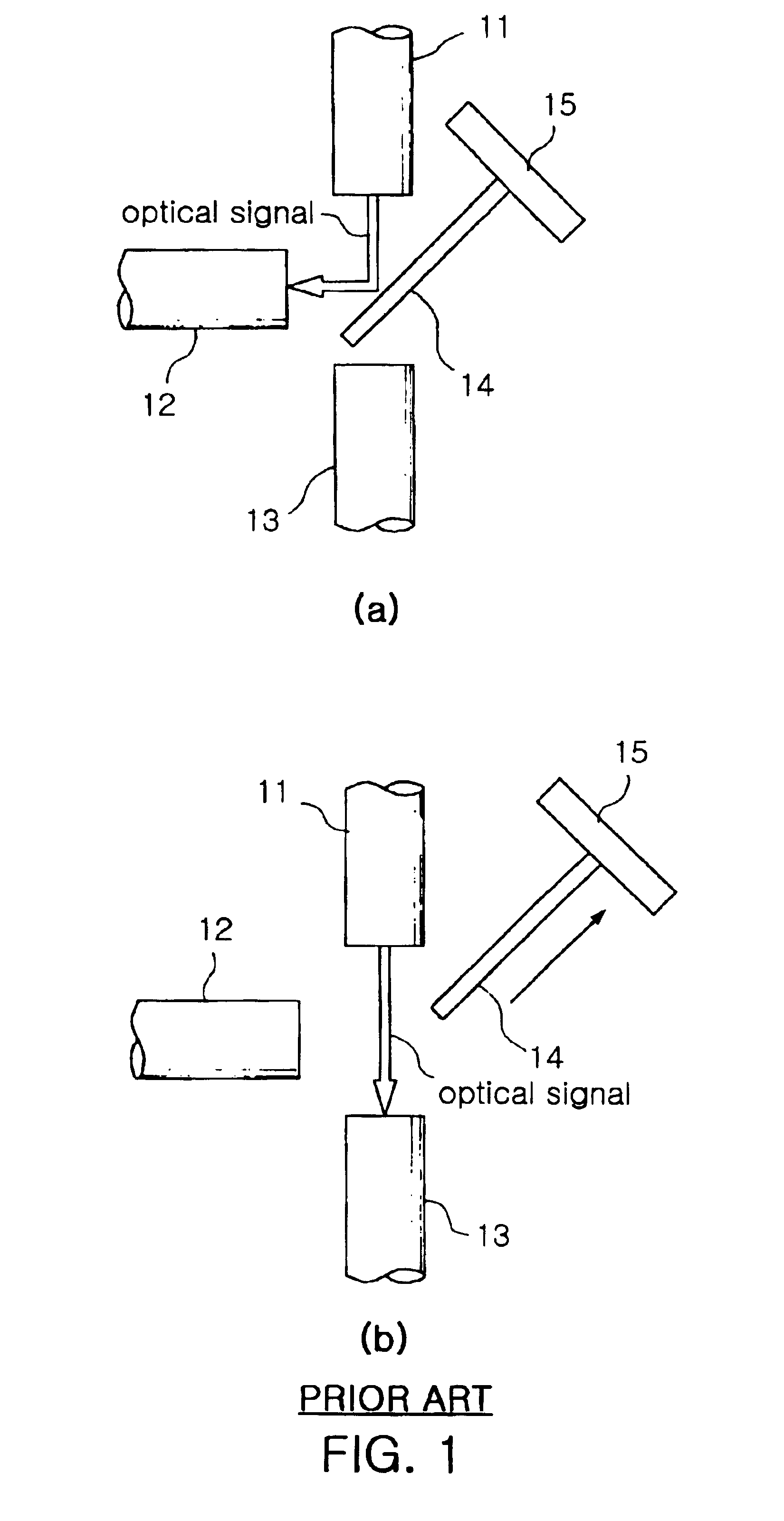
However, the MEMS optical switch has a cumbersome problem in that the input optical fiber and output optical fibers must be precisely arranged in a packaging process.
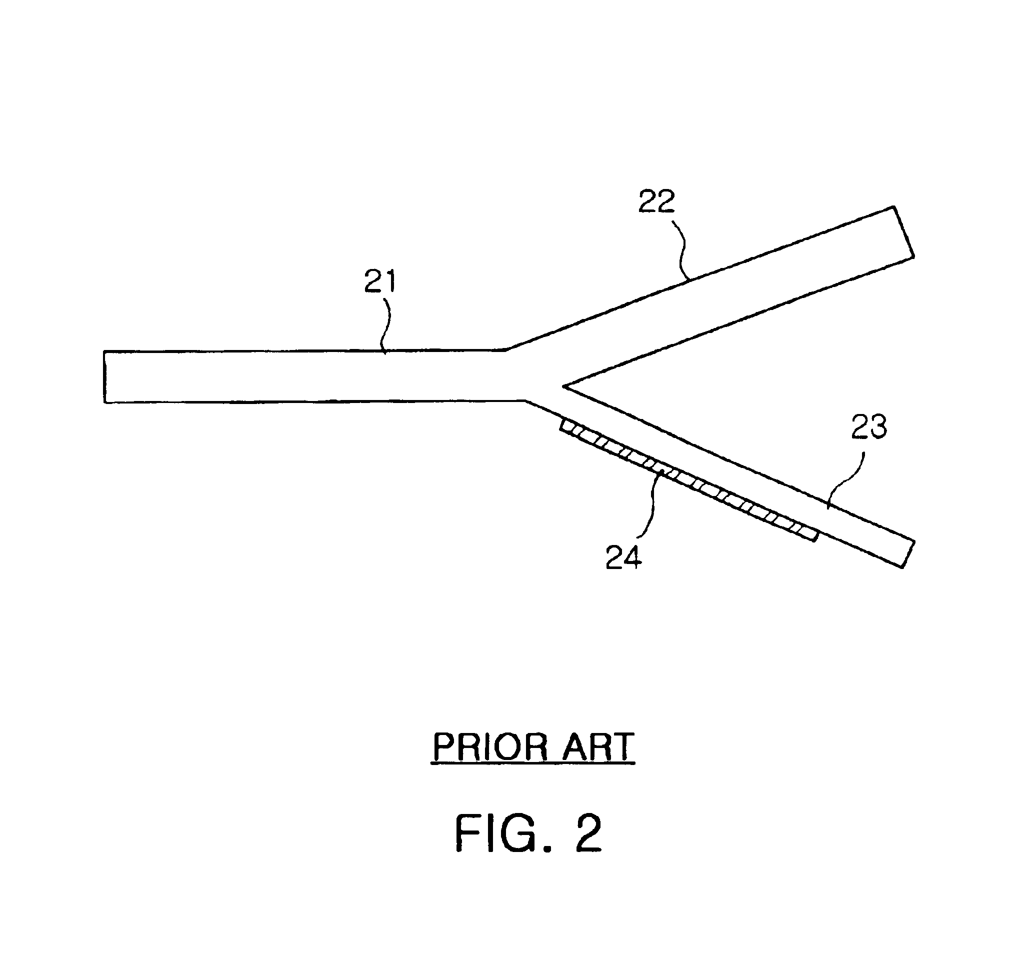
However, the conventional waveguide optical switch has disadvantages in that electric power is consumed in a large amount because heat energy is used to switch the path of the optical signal, and a switching speed is undesirably slow.
Method used
Image
Click on the blue label to locate the original text in one second.
Reading with bidirectional positioning of images and text.
Examples
first embodiment
[0027]FIGS. 3A and 3B illustrate an optical switch according to the present invention.
[0028]FIG. 3A illustrates the optical switch 30 in an offset state. The optical switch 30 includes an input waveguide 32 connected to an input optical fiber 31 through which an optical signal is inputted, a plurality of output waveguides 34a, 34b connected to two or more output optical fibers 33 through which the optical signal is outputted, a plurality of moving waveguides 35a, 35b for connecting the input waveguide 32 to the output waveguides 34a, 34b, and an actuator 37 provided with a fixed part 38 mounted on a predetermined base (not shown) and a moving part 36. At this time, the moving part 36 is connected to the fixed part 38 by a spring and assembled with the moving waveguides 35a, 35b. The moving part 36 perpendicularly moves by a predetermined force.
[0029]The input waveguide 32 and output waveguides 34a, 34b are fixedly installed on a wafer, and connected to an input optical fiber 31 and ...
second embodiment
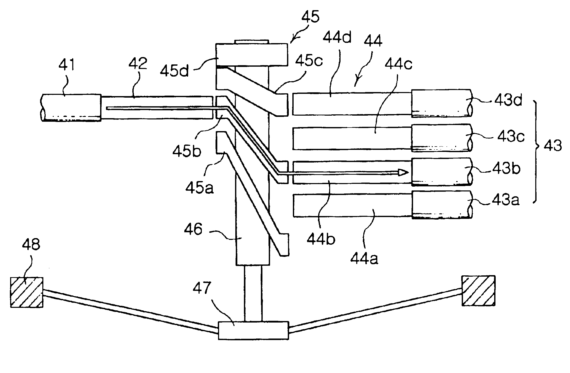
[0041]FIGS. 4A and 4B illustrate an optical switch having the four switching paths according to the present invention, in which optical signals of FIGS. 4A and 4B pass through the different switching paths.
[0042]The optical switch of FIGS. 4A and 4B includes an input waveguide 42 which does not move, four output waveguides 44a, 44b, 44c, 44d arranged in a direction toward which an actuator 47 moves, the actuator 47 connected to a fixed part 48 by a spring and having a moving part 46 perpendicularly moving by a predetermined force, and four moving waveguides 45a, 45b, 45c, 45d positioned at an upper part of the moving part 46 of the actuator 47 and arranged in a direction toward which the actuator 47 moves. At this time, the moving waveguides 45a, 45b, 45c, 45d perpendicularly move in such a way that the first ends of the moving waveguides 45a, 45b, 45c, 45d correspond in position to the input waveguide 42, and the second ends of the moving waveguides 45a, 45b, 45c, 45d correspond in...
third embodiment
[0048]FIGS. 5A and 5B illustrate an optical switch according to the present invention, in which a path of an optical signal is switched using an electrostatic force, usually used in a MEMS technology field.
[0049]In FIGS. 5A and 5B, a comb-shaped moving electrode 37a is formed at an end of the actuator 37 of FIG. 3, and a fixed electrode 37b is formed at a predetermined distance from the moving electrode 37a.
[0050]When a voltage is not applied to the moving electrode 37a and fixed electrode 37b, a moving part 36 does not move, and a first moving waveguide 35a is positioned between an input waveguide 32 and a first output waveguide 34a as shown in FIG. 5A.
[0051]On the other hand, when the voltage is applied to the moving electrode 37a and fixed electrode 37b, a predetermined voltage difference occurs between the moving electrode 37a and fixed electrode 37b to generate an electrostatic force, thus the moving electrode 37a and the moving part 36 integrally assembled with the moving ele...
PUM
Abstract
Disclosed is herein an optical switch, which has advantages of an MEMS optical switch and a waveguideoptical switch including a small electric power consumption, an easy packaging process, and a fast switching speed. The optical switch includes an input waveguide connected to an input optical fiber through which an optical signal is inputted, and a plurality of output waveguides connected to a plurality of output optical fibers through which the optical signal is outputted. An actuator is positioned between the input waveguide and the output waveguides, and has an MEMS structure including a fixed part and a moving part connected to the fixed part by a spring to move by a predetermined force. Additionally, a plurality of moving waveguides are assembled with the moving part of the actuator and move in the same direction as the movement of the moving part in such a way that first ends of the moving waveguides correspond in position to the input waveguide, and second ends of the moving waveguides correspond in position to the output waveguides.
Description
BACKGROUND OF THE INVENTION[0001]1. Field of the Invention[0002]The present invention relates, in general, to an optical switch used as essential parts of a wavelength division multiplexing (WDM) optical communications network and, more particularly, to an optical switch, which has a fast response speed, consumes a small amount of an electric power, and is useful in a precise and easy packaging process because it is possible to connect the optical switch to optical fibers according to a simple process, and a method of producing the same.[0003]2. Description of the Related Art[0004]Generally, an optical switch functions to change a path of an optical signal transmitted through an optical fiber in a WDM optical communications network, and current studies of the optical switch are being concentrated on an optical switch realized according to a micro electro mechanical systems (MEMS) technology and an optical switch realized using the refraction change due to heat energy.[0005]In an MEM...
Claims
Application Information
Patent Timeline
Application Date:The date an application was filed.
Publication Date:The date a patent or application was officially published.
First Publication Date:The earliest publication date of a patent with the same application number.
Issue Date:Publication date of the patent grant document.
PCT Entry Date:The Entry date of PCT National Phase.
Estimated Expiry Date:The statutory expiry date of a patent right according to the Patent Law, and it is the longest term of protection that the patent right can achieve without the termination of the patent right due to other reasons(Term extension factor has been taken into account ).
Invalid Date:Actual expiry date is based on effective date or publication date of legal transaction data of invalid patent.

