Liquid crystal display

Inactive Publication Date: 2005-07-14
SEIKO INSTR INC
View PDF2 Cites 0 Cited by
  • Summary
  • Abstract
  • Description
  • Claims
  • Application Information

AI Technical Summary

Benefits of technology

[0010] Further, the first layer wiring is made from a metal thin film such as aluminum so that parasitic capacitance is reduced since fine but low-resistance wiring can be made. Furthermore, low electric power consumption and high display quality are achieved since no portion of the first layer wiring other than the through-holes is overlapped with the second layer electrode.
[0011] In the configuration of the liquid crystal display according to the present invention, addition of only one process to a typical color filter manufacturing process enables a double-layer configuration in which the segment electrodes are divided into first-layer wirings and second-layer electrodes, and the panel can be driven divisionally at low duty. Accordingly, in comparison to the method of laminating the wiring electrode and the insulation film by the conventional divisional driving, a low-cost panel can be manufactured, and a liquid crystal display with improved display quality and reduced power consumption can be provided in comparison to a panel with high duty driving of an ordinary single layer electrode having the same number of pixels.

Problems solved by technology

Whichever driving method is used, increase of the number of common lines in a display area results in decrease of the ON / OFF ratio of the effective value of the driving voltage to be applied to the liquid crystal, thus reduction of contrast as well as slowing of response speed occurs.
In this configuration however there arises a problem of increase in manufacturing process coming from the fact that additional film formation and patterning are required for each wiring, electrode, and insulation film all of which are laminated.
Another problem in the aforementioned configuration is that the second layer electrode is formed on the first layer wiring, and thus a large parasitic capacitance is generated between the first layer wiring and the second layer electrode, consequently electric power consumption increases.
There arises a further problem in that signals applied to the first layer wiring and the second layer electrode are influenced with each other by the parasitic capacitance to distort waveforms, thereby giving different luminosity to each divided screen and degrading display quality.

Method used


Image

  • Liquid crystal display
  • Liquid crystal display
  • Liquid crystal display

Examples


Embodiment Construction

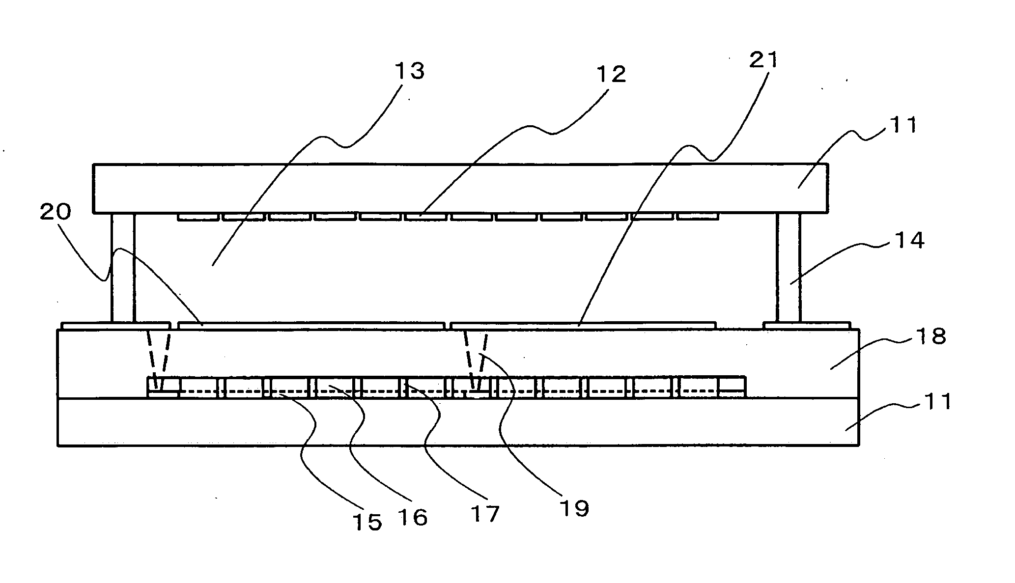
[0018]FIG. 5 shows an example of a liquid crystal display of the present invention, in which one liquid crystal panel is driven divisionally in the first screen 53 and in the second screen 54. FIG. 1 is a cross-sectional view showing the transparent liquid crystal display of the present invention, taken from the FIG. 5 along the line A-A′ of the panel 53 and 54.

[0019] At first aluminum is deposited by sputtering on a glass substrate 11 to which color filters are formed later and then the first layer wirings 15 are formed by patterning. When the aluminum thin film on pixel portions are left at this time as reflecting plates electrically separated from wiring electrodes, a semi-transparent liquid crystal panel will be made. Acrylic resin dispersed with pigment is applied on the reflecting plates by spinner, and then patterned. This process is repeated to form color filters 16 and black matrices 17. Acrylic resin is further applied on the color filters 16 and the black matrices 17 by ...


PUM


Abstract

A plurality of first layer wirings (15) and a plurality of second layer segment electrodes (20 and 21) are insulated by a plurality of color filters (16) and a smoothing film (18). A plurality of through-holes are formed in portions of a plurality of black matrices by patterning and then a plurality of second layer electrodes are formed, thereby connecting the plurality of first layer wirings to the plurality of second layer segment electrodes.

Description

BACKGROUND OF THE INVENTION [0001] 1. Field of the Invention [0002] The present invention relates to a structure of a passive matrix color liquid crystal display using super-twisted nematic (referred to as STN) liquid crystal etc., and more particularly, to a structure of a liquid crystal display whose display area is driven to have two or more divided screens. [0003] 2. Description of the Related Art [0004] A passive matrix liquid crystal display has a liquid crystal layer interposed between a common electrode substrate and a segment electrode substrate and pixels arranged in matrix. Examples of a driving method for a passive matrix type liquid crystal display include a voltage averaging method, smart addressing (SA) method, and multi line addressing (MLA) method. [0005] Whichever driving method is used, increase of the number of common lines in a display area results in decrease of the ON / OFF ratio of the effective value of the driving voltage to be applied to the liquid crystal, ...

Claims


Application Information

Patent Timeline
IPC IPC(8): G02F1/1335G02F1/1333G02F1/1343
CPCG02F1/133516G02F2001/133357G02F1/134327G02F1/133357
Inventor HOSHINO, MASAFUMI
Owner SEIKO INSTR INC
Why Eureka
Try Eureka