High noise rejection voltage-controlled ring oscillator architecture

a ring oscillator and high noise rejection technology, applied in the direction of electric pulse generators, automatic control of pulses, amplifiers, etc., can solve the problems of reducing the accuracy of the pll and the ability to reject noise, so as to improve the noise rejection level, and reduce the coupling of noise

Inactive Publication Date: 2005-11-08
AVAGO TECH WIRELESS IP SINGAPORE PTE
View PDF22 Cites 4 Cited by
  • Summary
  • Abstract
  • Description
  • Claims
  • Application Information

AI Technical Summary

Benefits of technology

[0012]The ring oscillator circuit of the present invention provides an improved level of noise rejection over prior art VCO circuits because the inventive differential delay circuit rejects noise originating from both the voltage supply and ground. Specifically, the first and second current sources reduce the coupling of noise from the first power supply terminal to the output, while the third current source reduces the coupling of noise from the second power supply terminal to the output.

Problems solved by technology

The coupling of noise to the VCO 100 causes the output signal VCO—out to suffer from jitter (i.e., rapid variations in phase), thereby reducing the accuracy of the PLL.
A disadvantage of the differential inverters 210 and 310 is that they are capable of rejecting noise from only one of the potential switching noise sources VDD and ground, but not both.

Method used


Image

  • High noise rejection voltage-controlled ring oscillator architecture
  • High noise rejection voltage-controlled ring oscillator architecture
  • High noise rejection voltage-controlled ring oscillator architecture

Examples


Embodiment Construction

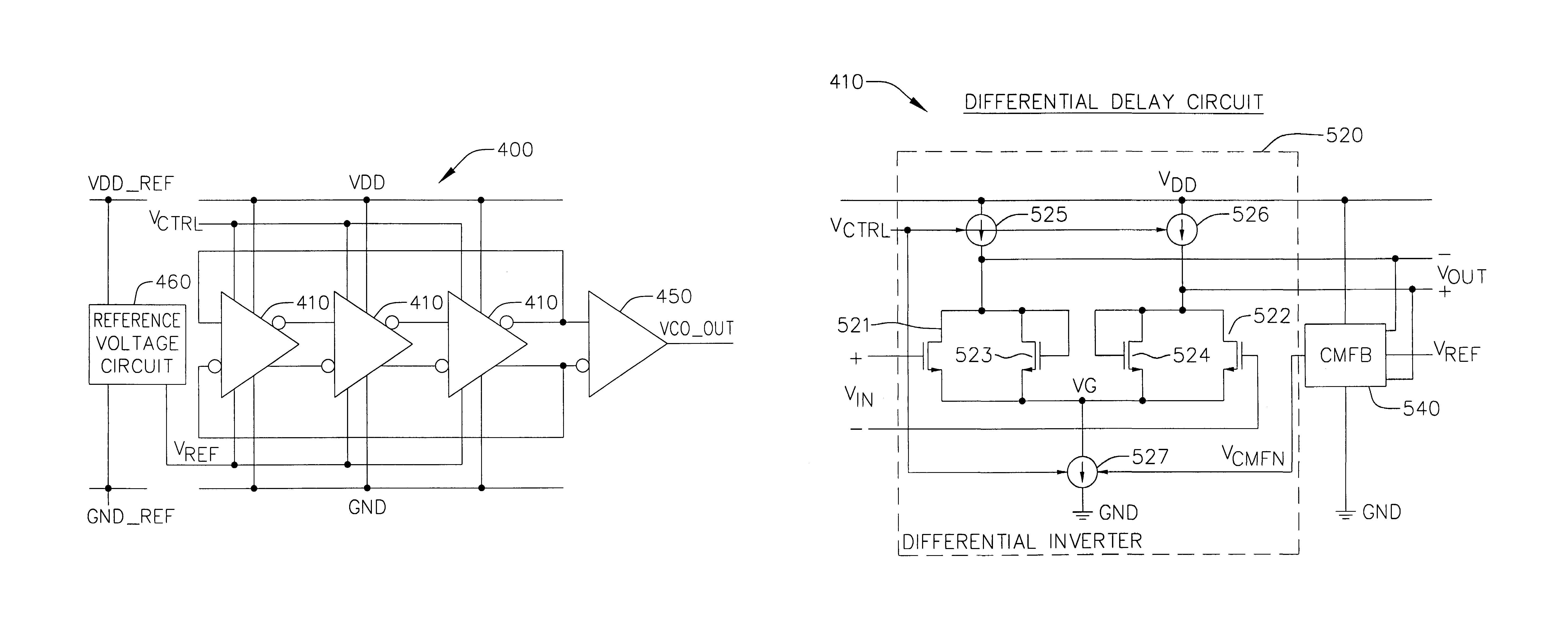
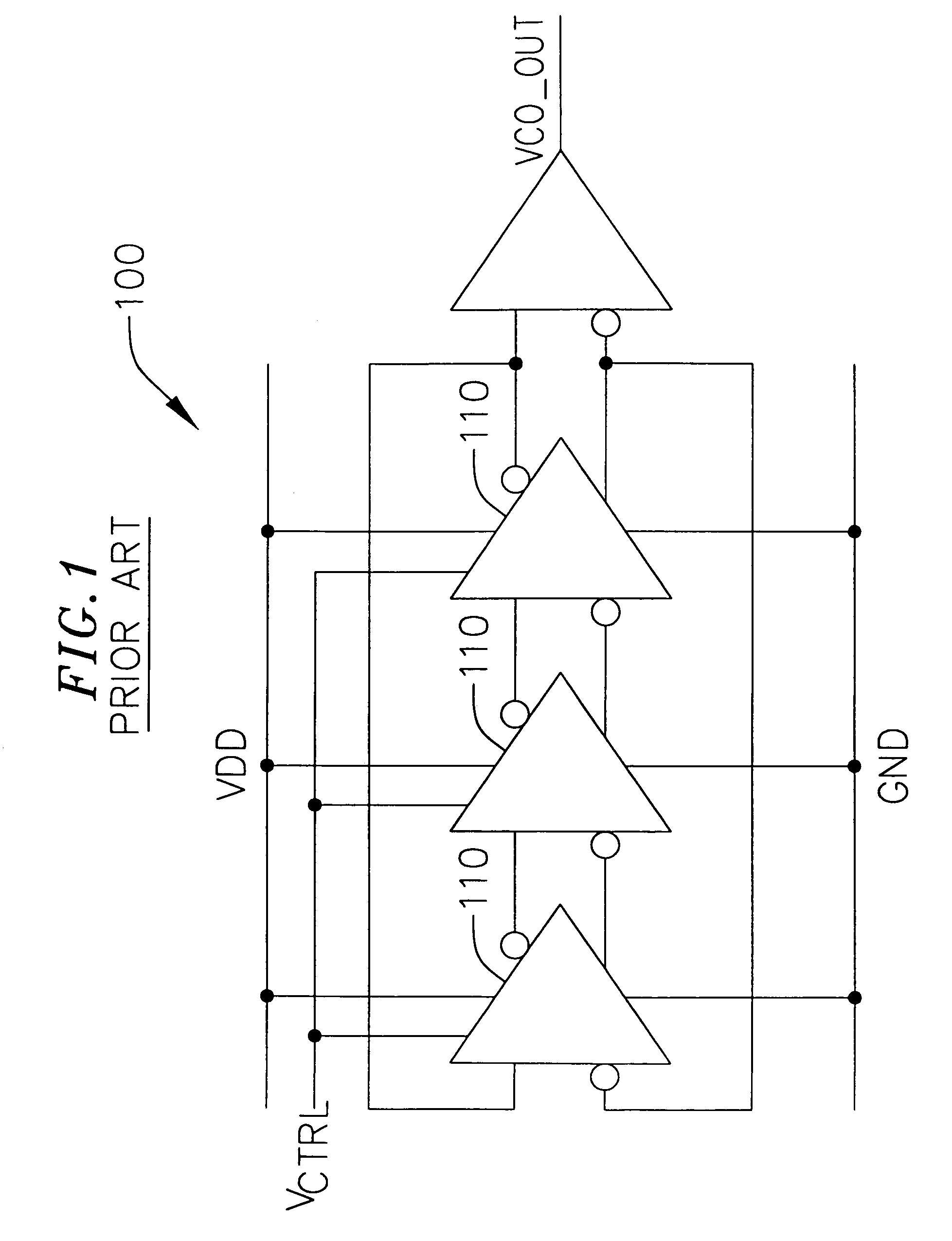
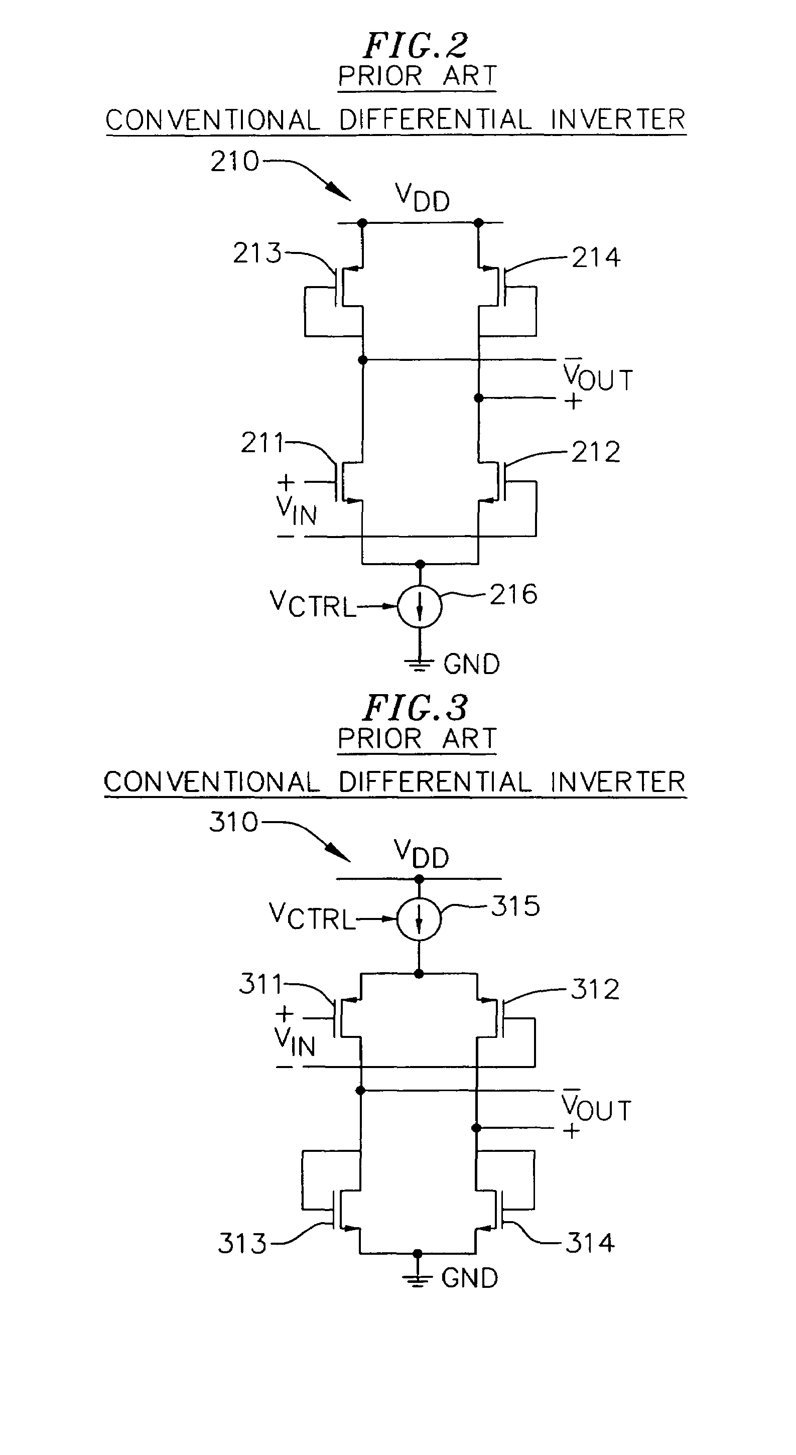
[0018]The present invention comprises a ring oscillator circuit, such as a VCO, with an improved level of noise rejection for noise originating from both the voltage supply and ground, i.e., an improved PSRR. As a result, the output signal generated by the ring oscillator circuit suffers from less jitter than conventional ring oscillator or VCO circuits in the presence of such noise. Consequently, the ring oscillator of the present invention is especially suitable for use as a VCO in integrated circuits that include digital circuits, such as microprocessors or digital signal processors (DSPs). The following description is presented to enable any person skilled in the art to make and use the invention, and is provided in the context of a particular application and its requirements. Various modifications to the preferred embodiment will be readily apparent to those skilled in the art, and the generic principles defined herein may be applied to other embodiments and applications withou...


PUM


Abstract

A ring oscillator circuit, such as a VCO, with a relatively high level of noise rejection for noise originating from both the voltage supply and ground. The ring oscillator circuit is composed of a plurality of differential delay circuits, each differential delay circuit generating a differential output signal that is a delayed (and preferably inverted) version of a differential input signal. ‘Each differential delay circuit includes first and second input transistors for receiving the differential input signal. Each differential delay circuit also includes first and second load transistors coupled in parallel with the respective first and second input transistors. Each differential delay circuit further includes a first current source coupled between the first input transistor and a first power supply terminal (e.g., a voltage supply terminal), a second current source coupled between the second input transistor and the first power supply terminal and a third current source coupled between the first and second input transistors and a second power supply terminal (e.g., a ground terminal). The first and second current sources reduce the coupling of noise from the first power supply terminal to the output. The third current source reduces the coupling of noise from the second power supply terminal to the output.

Description

CROSS-REFERENCE TO RELATED APPLICATIONS[0001]This application is a continuation of U.S. patent application Ser. No. 10 / 679,839, filed Oct. 6, 2003, now U.S. Pat. No. 6,828,866 and entitled “High Noise Rejection Voltage-Controlled Ring Oscillator Architecture,” which is a continuation of U.S. patent application Ser. No. 10 / 131,963, filed Apr. 25, 2002, now issued as U.S. Pat. No. 6,657,503, which is a continuation of U.S. patent application Ser. No. 09 / 507,114, filed Feb. 17, 2000, now issued as U.S. Pat. No. 6,414,557, all of which are incorporated herein by reference.BACKGROUND OF THE INVENTION[0002]1. Field of the Invention[0003]This invention relates generally to ring oscillator circuits and, in particular, to a ring oscillator or VCO circuit that provides an improved level of noise rejection for noise originating from both the voltage supply and ground.[0004]2. Description of the Related Art[0005]High-speed digital circuits such as microprocessors and memories often employ a pha...

Claims


Application Information

Patent Timeline
Patent Type & Authority Patents(United States)
IPC IPC(8): H03K5/13H03K3/0231H03F3/72H03L7/08H03F3/45H03K3/00H03L7/099H03K5/00
CPCH03F3/45183H03F3/4565H03F3/72H03K3/0231H03K5/133H03L7/0995H03K3/0322H03F2203/7203H03K2005/00208
Inventor LIU, BIN
Owner AVAGO TECH WIRELESS IP SINGAPORE PTE
Why Eureka
Try Eureka