Method of manufacturing thin film piezoelectric element, and element housing jig

a piezoelectric element and manufacturing method technology, applied in the direction of piezoelectric/electrostrictive transducers, transducer types, electrical transducers, etc., can solve the problems of difficult discrimination from this inspection, difficult to further improve the accuracy of head positioning, and individual inspection of separated piezoelectric elements, etc., to achieve excellent effects and improve yield and mass-productivity of thin film elements

Active Publication Date: 2005-11-15
TDK CORPARATION
View PDF7 Cites 3 Cited by
  • Summary
  • Abstract
  • Description
  • Claims
  • Application Information

AI Technical Summary

Benefits of technology

[0008]The present invention is intended to solve the above problems, and a purpose of the invention is to provide a method of manufacturing thin film piezoelectric elements such that the thin film piezoelectric elements do not come into contact with each other in a chemical solution tank or a cleaning tank, whereby the thin film piezoelectric elements can be prevented from being damaged, and such that operations to handle the piezoelectric elements in the solution tank and to remove them from the solution tank are facilitated, thereby improving workability and greatly enhancing yield. Another purpose of the invention is to provide an element housing jig used for manufacturing the thin film piezoelectric elements.
[0014]By this manufacturing method, when the thin film piezoelectric elements are separated from the substrate, it is possible to house the piezoelectric elements in a state of being isolated from each other. As a result, the thin film piezoelectric elements can be prevented from coming into contact with each other and being damaged. Also, since an arrangement of the thin film piezoelectric elements can be maintained as it is on the substrate, only non-defective ones of the piezoelectric elements can be mounted by chucking them from the element housing jig in accordance with a result of characteristic inspection of the piezoelectric elements while on the substrate. Accordingly, it is possible to greatly improve mass-productivity of thin film piezoelectric elements and to enhance yield thereof.
[0018]With this configuration, it is possible to individually and separately hold the thin film elements with respect to each other after the thin film elements have been separated from a substrate, which thin film elements can be and used as thin film piezoelectric elements. Accordingly, the element housing jig of the present invention will bring about excellent effects such as considerable improvement of yield and mass-productivity of thin film elements.

Problems solved by technology

However, with a configuration in which the actuator arm is rotated by the VCM for positioning the head, it is very difficult to further improve head positioning accuracy.
Also, after the thin film piezoelectric elements 80 are inspected on the substrate 91, if they are separated into individual pieces in the chemical solution tank, it will make discrimination from this inspection difficult.
Therefore, there arises a problem in that the separated piezoelectric elements must be individually inspected.
Further, it is difficult to automate an operation to remove the thin film piezoelectric elements 80, as loose pieces, from the chemical solution tank or a cleaning tank.

Method used


Image

  • Method of manufacturing thin film piezoelectric element, and element housing jig
  • Method of manufacturing thin film piezoelectric element, and element housing jig
  • Method of manufacturing thin film piezoelectric element, and element housing jig

Examples


first exemplary embodiment

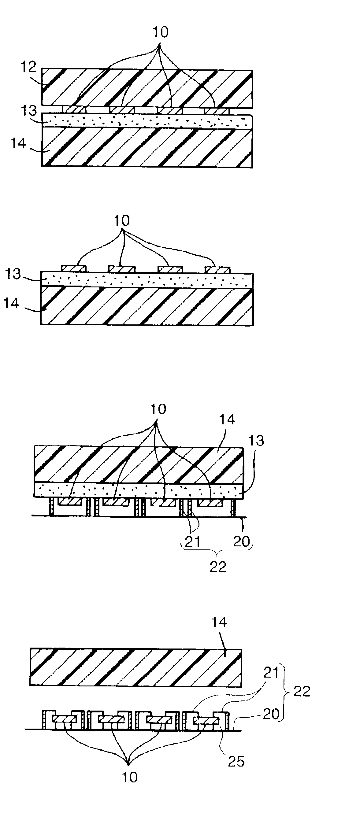
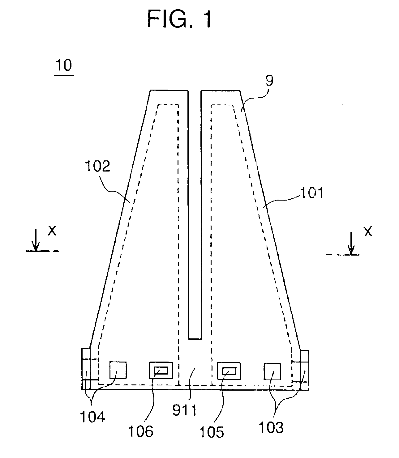
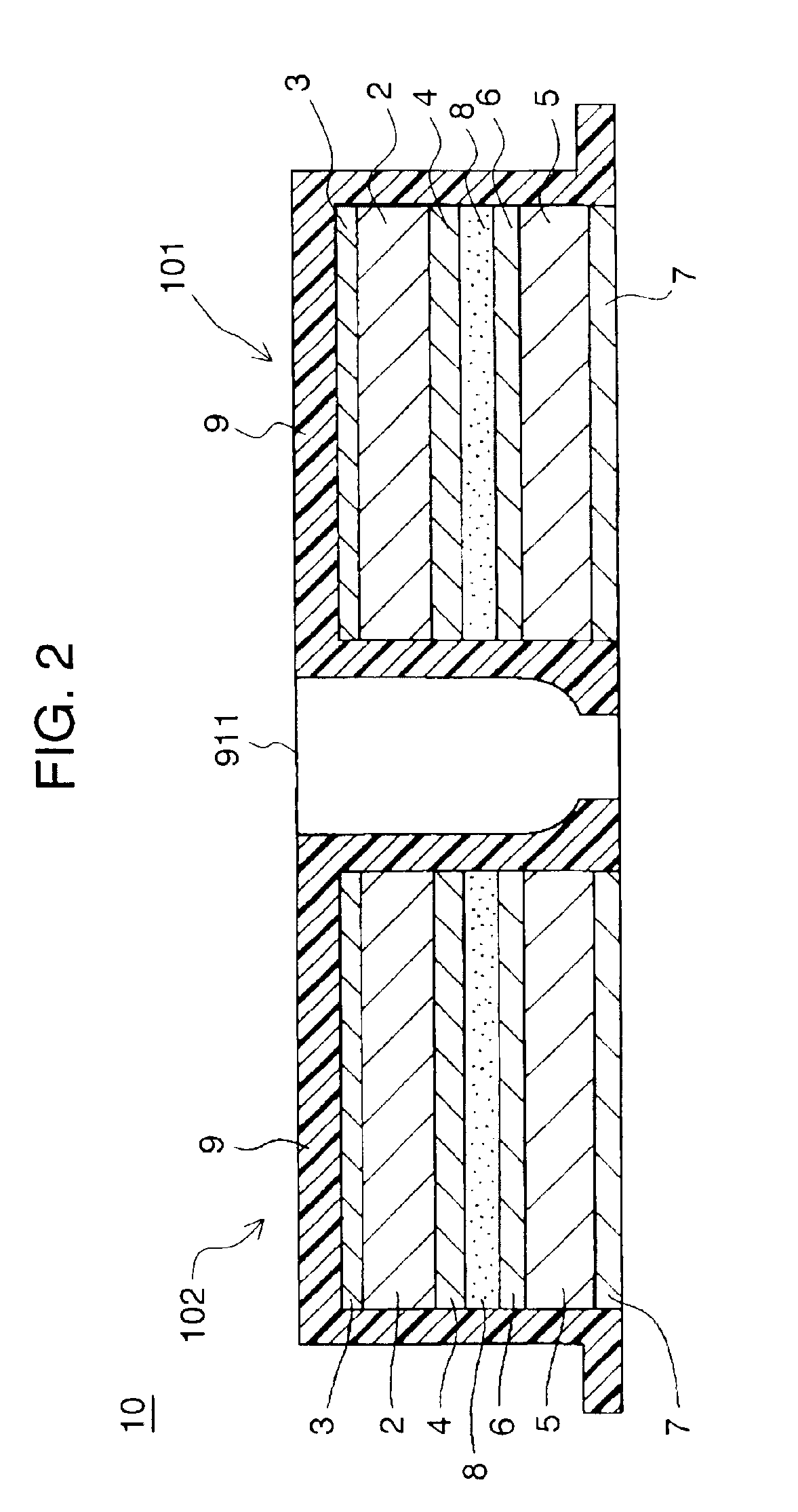
[0048]FIG. 1 is a plan view showing an example of paired thin film piezoelectric elements formed by a manufacturing method of a first exemplary embodiment of the present invention. Also, FIG. 2 is a sectional view along the X—X line of FIG. 1. By using these figures, structure of a thin film piezoelectric element 10 is briefly explained in the following. In the thin film piezoelectric element 10, a right piezoelectric element 101 and a left piezoelectric element 102, which are symmetrical with regard to one another, are covered with coating resin 9.

[0049]As shown in FIG. 2, the right piezoelectric element 101 and the left piezoelectric element 102, forming the thin film piezoelectric element 10, are each formed of a laminate structure including a first thin film piezoelectric material 2 and a second thin film piezoelectric material 5. The first thin film piezoelectric material 2 is provided with a first electrode layer 3 and a third electrode layer 4 formed on opposite surfaces ther...

second exemplary embodiment

[0071]In a second exemplary embodiment, a manufacturing method to be described is such that a temporary fixing substrate is provided with slits corresponding to projections of an element housing jig, and by using the temporary fixing substrate, thin film piezoelectric elements are separated from the substrate and housed in the element housing jig. Also in the present exemplary embodiment, description will be given with respect to a case of paired thin film piezoelectric elements as described with regard to the first exemplary embodiment. The same elements as those in FIG. 1 to FIG. 6B are given same reference numerals.

[0072]FIG. 7 is a plan view of temporary fixing substrate 34 provided with slits 341 corresponding to partition walls 21, which are projections of the element housing jig 22 used in the first exemplary embodiment. FIG. 8A to FIG. 8D are sectional views for description of steps during which thin film piezoelectric elements 10 are separated by using the temporary fixing ...

third exemplary embodiment

[0079]A third exemplary embodiment of the present invention is a manufacturing method in which an adhesive layer is removed by etching while a temporary fixing substrate is pressed in a direction of an element housing section, and an element housing jig formed from the temporary fixing substrate is employed

[0080]FIG. 9A is a sectional view showing a state of temporary fixing substrate 44 with thin film piezoelectric elements 10 bonded thereto by adhesive layer 130 before being combined with element housing jig 350. The thin film piezoelectric elements 10 are bonded by the adhesive layer 130 onto the temporary fixing substrate 44. The temporary fixing substrate 44 is provided with lengthwise slits 441, widthwise slits 442, and openings 443 for improving flow of a solution, which will be described later in detail.

[0081]The element housing jig 350 comprises two-stage reinforcing plates 301, posts 302 for fixing the reinforcing plates 301, and element housing portions 220. The reinforci...


PUM

PropertyMeasurementUnit
thicknessaaaaaaaaaa
thicknessaaaaaaaaaa
thicknessaaaaaaaaaa

Abstract

A method comprises: bonding a plurality of thin film piezoelectric elements, formed on a substrate, onto a temporary fixing substrate via an adhesive layer; selectively removing the substrate to expose the thin film piezoelectric elements; fixing an element housing jig having sectional regions for individually isolating the thin film piezoelectric elements in such manner that the thin film piezoelectric elements and the sectional regions correspond to each other; and dissolving and removing the adhesive layer, and housing the thin film piezoelectric elements in the sectional regions of the element housing jig. Accordingly, it is possible to individually isolate and house the thin film piezoelectric elements removed from the substrate.

Description

FIELD OF THE INVENTION[0001]The present invention relates to a method of manufacturing a thin film piezoelectric element for an actuator used for positioning a head, or the like, of a disk recording and reproducing apparatus (hereinafter called disk unit), and an element housing jig used for manufacturing the thin film piezoelectric element.BACKGROUND OF THE INVENTION[0002]In recent years, disk recording density of a disk unit has been increased at a rate of 10% per year. A head for recording and reproducing data on a disk is generally mounted on a slider. The slider with a head mounted thereon is fixed to a side opposing the disk at one end of an actuator arm. At another end of the actuator arm is disposed a voice coil motor (hereinafter called VCM). The actuator arm is rotated by the VCM, thereby positioning the head to a predetermined track position of the disk for performing a recording or reproducing operation.[0003]For recording data on a disk at higher densities, it is necess...

Claims


Application Information

Patent Timeline
Patent Type & Authority Patents(United States)
IPC IPC(8): H01L41/22
CPCH01L41/313H01L41/316Y10T29/49126Y10T29/42H10N30/073H10N30/076
Inventor MIKAMI, HIROSUKEUCHIYAMA, HIROKAZUKUWAJIMA, HIDEKI
Owner TDK CORPARATION
Why Eureka
Try Eureka