Method of fabricating vertical one-transistor floating-body DRAM cell in bulk CMOS process with electrically isolated charge storage region

a floating-body dram cell and bulk cmos technology, applied in the direction of transistors, electrical equipment, semiconductor devices, etc., can solve the problems of large area required for formation, requiring the use of pd-soi process, and relatively expensiv

Inactive Publication Date: 2005-11-15
MOSYS INC
View PDF11 Cites 60 Cited by
  • Summary
  • Abstract
  • Description
  • Claims
  • Application Information

AI Technical Summary

Benefits of technology

[0019]A recessed region is etched in the STI region adjacent to the semiconductor island region, wherein the recessed region extends a second depth below the upper surface of the substrate. The second depth is less than the first depth (i.e., the recessed region does not extend to the bottom of the STI region). The step of etching the recessed region exposes one or more sidewalls of the semiconductor island region. The top interface of the buried source region is located above the second depth, thereby enabling the formation of a vertical transistor along the sidewalls of the recessed region.

Problems solved by technology

Moreover, significant area is required to form the capacitor needed for storage of signal charge.
One significant disadvantage of conventional 1T / FB DRAM cell 100 is that it requires the use of partially depleted silicon-on-insulator (PD-SOI) process, which is relatively expensive and not widely available.
In addition, the floating body effect of the SOI process, although utilized in the 1T / FB DRAM cell advantageously, complicates circuit and logic designs significantly and often requires costly substrate connections to eliminate undesired floating body nodes not located in the 1T / FB DRAM cells.
Further, with a PD-SOI process, the device leakage characteristics can be difficult to control due to the lack of effective back-gate control of the bottom interface of the silicon layer that includes silicon regions 107–109.

Method used


Image

  • Method of fabricating vertical one-transistor floating-body DRAM cell in bulk CMOS process with electrically isolated charge storage region
  • Method of fabricating vertical one-transistor floating-body DRAM cell in bulk CMOS process with electrically isolated charge storage region
  • Method of fabricating vertical one-transistor floating-body DRAM cell in bulk CMOS process with electrically isolated charge storage region

Examples


Embodiment Construction

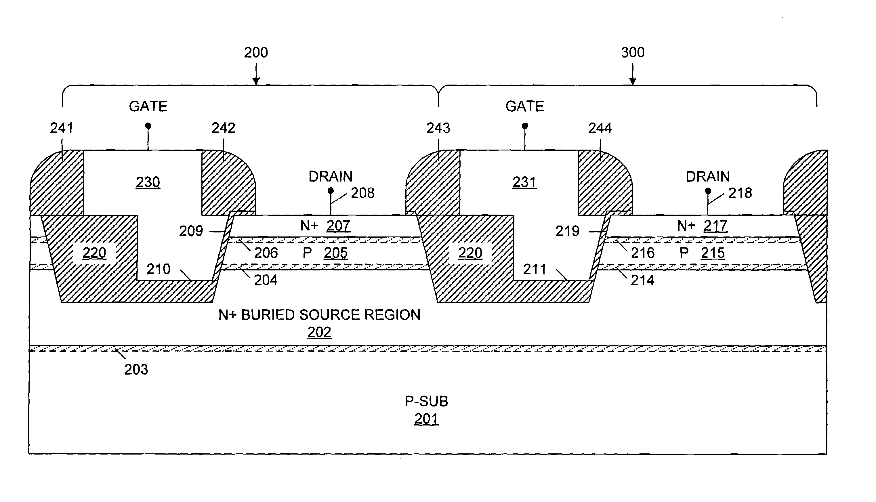
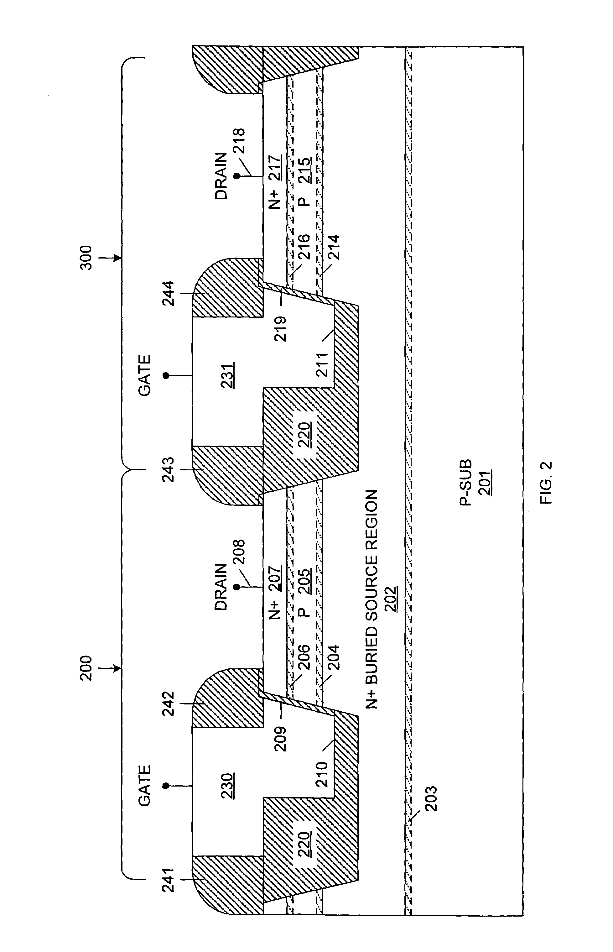
[0030]FIG. 2 is a cross-sectional view of two NMOS 1T / FB DRAM cells 200, 300 in accordance with one embodiment of the present invention. Although the present embodiment describes 1T / FB DRAM cells that use NMOS transistors, it is understood that either NMOS or PMOS transistors can be used to form 1T / FB DRAM cells in accordance with the present invention. When a PMOS transistor is used to implement the 1T / FB DRAM cell, the conductivity types of the various elements are reversed.

[0031]DRAM cells 200 and 300 share P− type silicon substrate 201, N+ type buried source region 202, depletion region 203 and shallow trench isolation (STI) region 220. As will become more apparent in view of the following description, the illustrated portions of STI region 220 are continuous outside of the cross-section illustrated by FIG. 2.

[0032]1T / FB DRAM cell 200 also includes P type floating body region 205, depletion regions 204 and 206, heavily-doped N++ type drain region 207, drain contact 208, gate oxi...


PUM


Abstract

A vertical one-transistor, floating-body DRAM cell is fabricated by forming an isolation region in a semiconductor substrate, thereby defining a semiconductor island in the substrate. A buried source region is formed in the substrate, wherein the top/bottom interfaces of the buried source region are located above/below the bottom of the isolation region, respectively. A recessed region is etched into the isolation region, thereby exposing sidewalls of the semiconductor island, which extend below the top interface of the buried source region. A gate dielectric is formed over the exposed sidewalls, and a gate electrode is formed in the recessed region, over the gate dielectric. A drain region is formed at the upper surface of the semiconductor island region, thereby forming a floating body region between the drain region and the buried source region. Dielectric spacers are formed adjacent to the gate electrode, thereby covering exposed edges of the gate dielectric.

Description

RELATED APPLICATIONS[0001]The present invention is a divisional of commonly owned U.S. patent application Ser. No. 10 / 095,984 filed Mar. 11, 2002, now U.S. Pat. No. 6,686,624, by Fu-Chieh Hsu, which is related to commonly owned, co-filed U.S. patent application Ser. No. 10 / 095,901, entitled “ONE-TRANSISTOR FLOATING-BODY DRAM CELL IN BULK CMOS PROCESS WITH ELECTRICALLY ISOLATED CHARGE STORAGE REGION” by Fu-Chieh Hsu.BACKGROUND OF THE INVENTION[0002]1. Field of the Invention[0003]The present invention relates to a dynamic random access memory (DRAM) cell, as well as methods for operating and fabricating a DRAM cell. More specifically, the present invention relates to a vertical one-transistor floating-body DRAM cell formed using a process compatible with a bulk CMOS process, wherein charge is stored inside an electrically isolated body region adjacent to the transistor channel region.[0004]2. Related Art[0005]Conventional one-transistor, one-capacitor (1T / 1C) DRAM cells require a comp...

Claims


Application Information

Patent Timeline
Patent Type & Authority Patents(United States)
IPC IPC(8): H01L27/108H01L21/70H01L21/8242
CPCH01L27/108H01L27/10802H01L29/7841H01L27/10823H01L27/10876H01L27/10891H10B12/20H10B12/34H10B12/00H10B12/053H10B12/488
Inventor HSU, FU-CHIEH
Owner MOSYS INC
Why Eureka
Try Eureka