Multi-layer substrates and fabrication processes

a technology of multi-layer substrates and fabrication processes, applied in the direction of printed circuits, programmable/customizable/modifiable circuits, printed element electric connection formation, etc., can solve the problems of significant loss of assembly space, significant space consumed by vias of this type, and interference with reliable connections, etc., to facilitate customization of vertical interconnections

Inactive Publication Date: 2005-11-15
TESSERA INC
View PDF52 Cites 50 Cited by
  • Summary
  • Abstract
  • Description
  • Claims
  • Application Information

AI Technical Summary

Benefits of technology

[0013]At least one of these steps is controlled so as to selectively control the connections between conductive features on different substrates provided by said leads. For example, the selective control may be provided by controlling the bond-making step, or by controlling the formation of connections between the lead fixed ends and conductive features on the substrate which initially carries the first set of leads. Also, the leads may be selectively provided or omitted. As further explained below, the steps required for selective control of the connections provided by the leads can be performed by treating, forming or removing features on the surface of the substrate. The process facilitates customization of the vertical interconnections.
[0014]In further processes according to other aspects of the invention, a component formed by joining

Problems solved by technology

In particular, because the adhesives on the connecting layers are activated at the same time as the conductive bonding materials used to make the electrical connections, the adhesives can be introduced into the electrical connections and can interfere with relia

Method used


Image

  • Multi-layer substrates and fabrication processes
  • Multi-layer substrates and fabrication processes
  • Multi-layer substrates and fabrication processes

Examples


Embodiment Construction

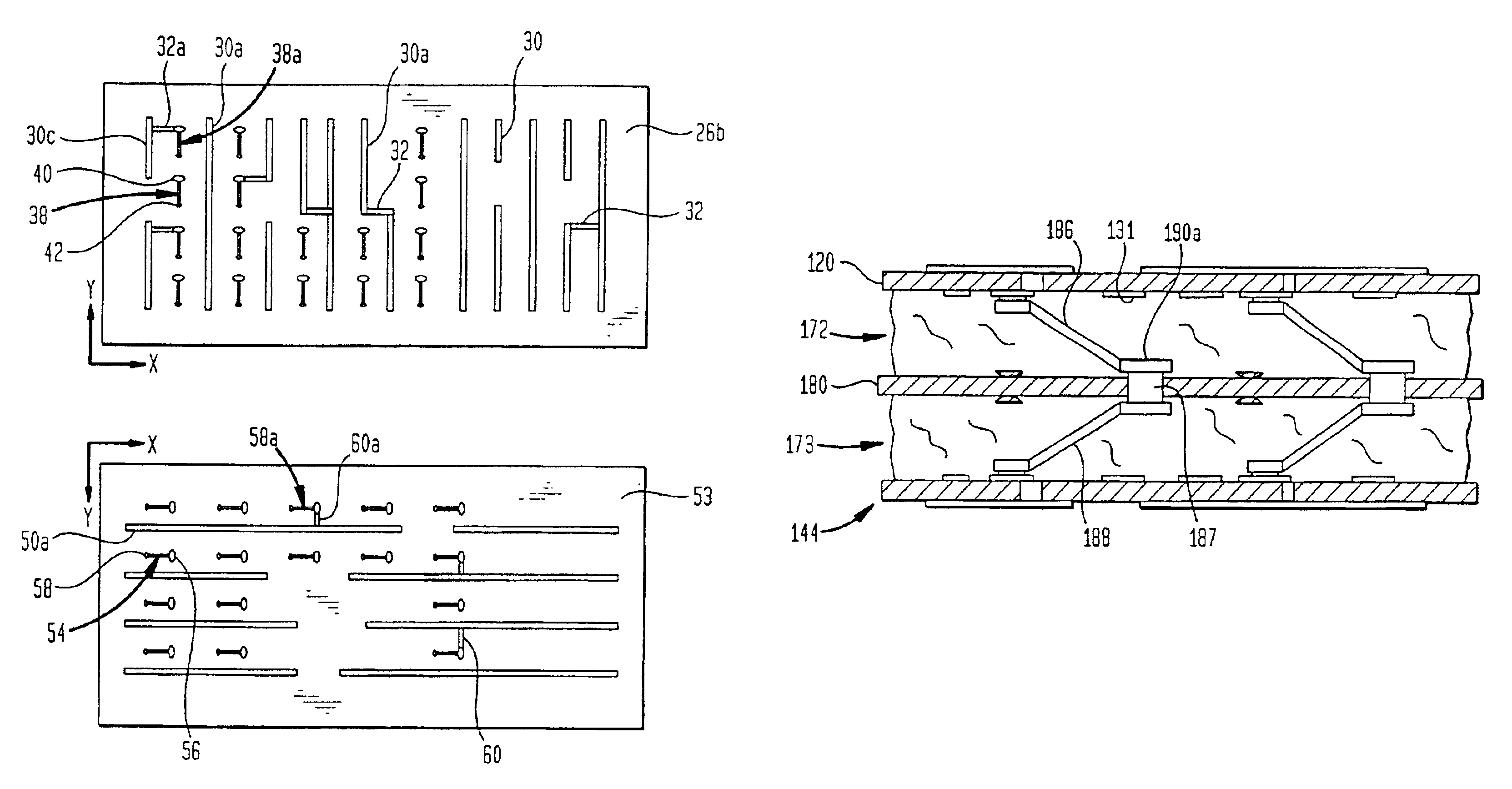
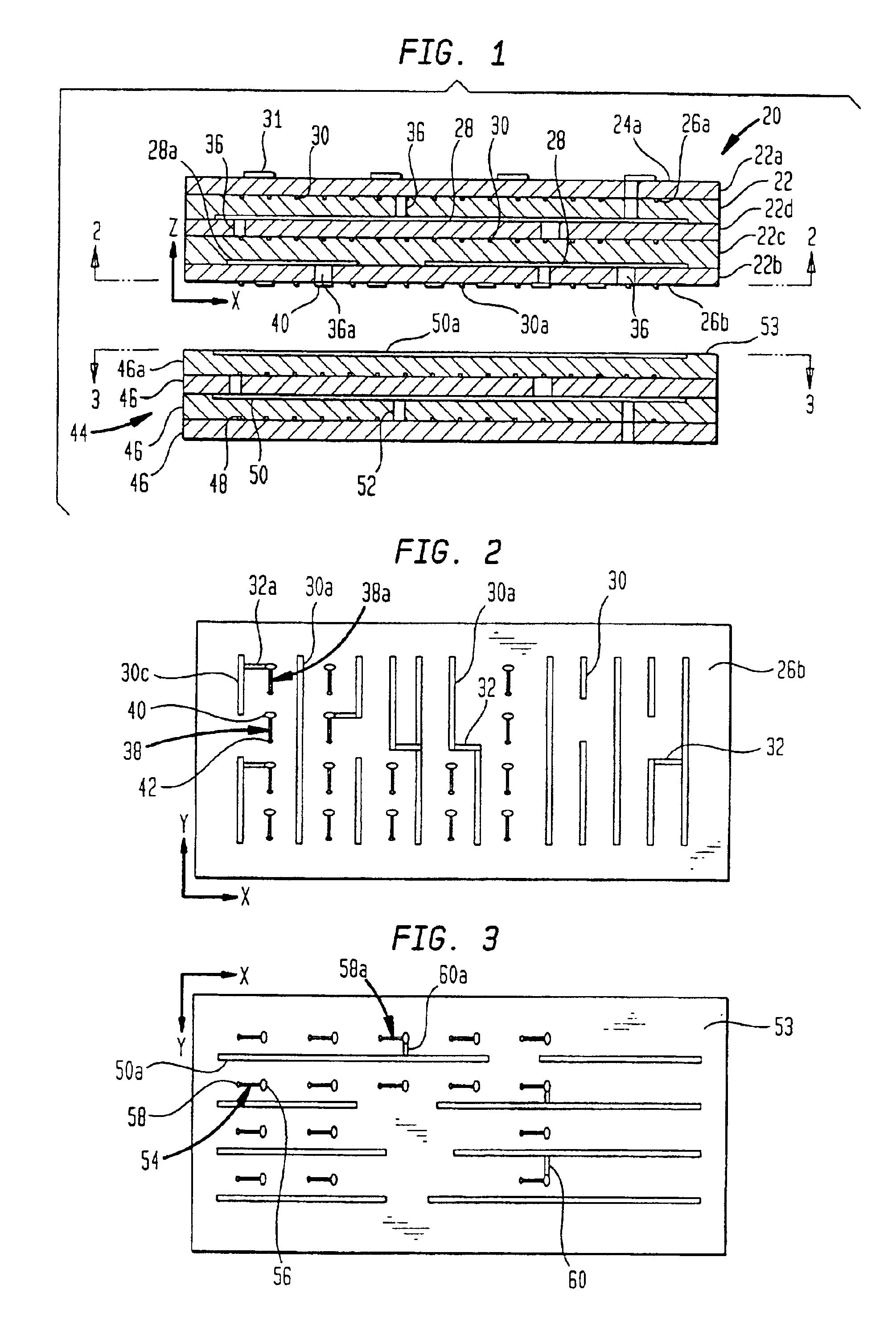
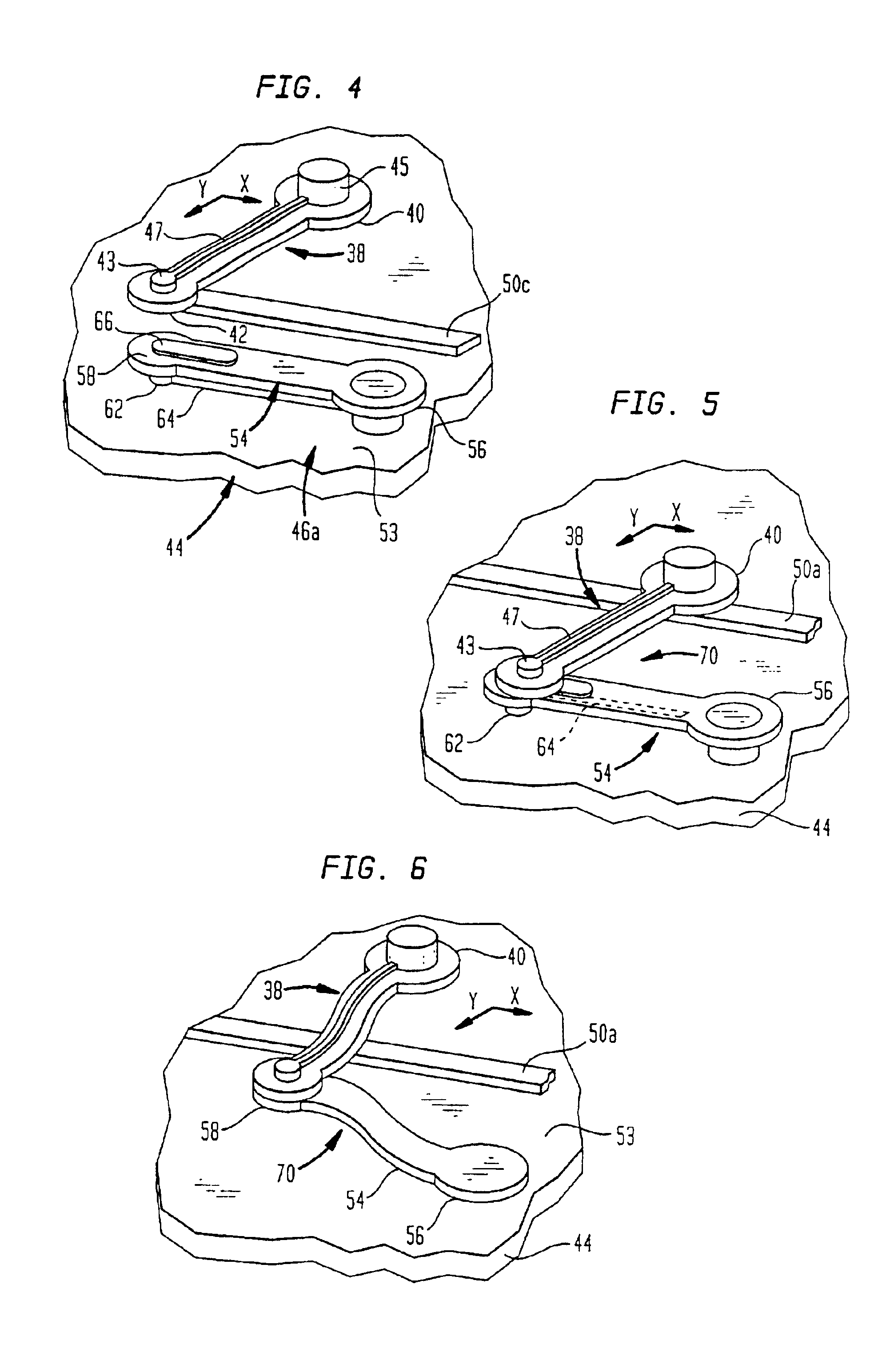
[0027]A substrate 20 in accordance with one embodiment of the invention includes several dielectric layers 22. In this embodiment, dielectric layers 22 are formed from polyimide. Each dielectric layer has a top surface 24 and a bottom surface 26 extending parallel to the top surface. The dielectric layers are superposed on one another so that the top surface of each dielectric layer other than the topmost dielectric layer 22a confronts the bottom surface of the next dielectric layer. The top surface 24a of the topmost dielectric layer is exposed at the top of the stack, whereas the bottom surface 26b of the bottom dielectric layer 22b is exposed at the bottom of the stack. The stacked dielectric layers define horizontal directions x and y (FIGS. 1 and 2). The stacked dielectric layers also define a vertical or z direction (FIG. 1) perpendicular to the x and y directions and perpendicular to the surfaces of layers 22. Substrate 20 includes layers of traces 28 extending principally in...


PUM


Abstract

Multi-layer components such as circuit panels are fabricated by connecting conductive features such as traces one two or more superposed substrates using leads extending through an intermediate dielectric layer. The leads can be closely spaced to provide a high density vertical interconnection, and can be selectively connected to provide customization of the structure.

Description

CROSS-REFERENCE TO RELATED APPLICATIONS[0001]The present application is a continuation of U.S. patent application Ser. No. 09 / 271,688, filed Mar. 18, 1999 now U.S. Pat. No. 6,429,112, which application is a continuation-in-part of U.S. patent application Ser. No. 09 / 138,858 filed Aug. 24, 1998 now U.S. Pat. No. 6,104,087, which in turn is a divisional of U.S. patent application Ser. No. 08 / 440,665, filed May 15, 1995, now U.S. Pat. No. 5,801,441, which in turn is a divisional of U.S. patent application Ser. No. 08 / 271,768, filed Jul. 7, 1994, now U.S. Pat. No. 5,518,964. Said application Ser. No. 09 / 271,688 is also a continuation-in-part of U.S. patent application Ser. No. 08 / 712,855, filed Sep. 12, 1996 now U.S. Pat. No. 6,191,368, which application claims benefit of U.S. Provisional Patent Application Ser. No. 60 / 003,619, filed Sep. 12, 1995. Said application Ser. No. 09 / 271,688 is also a continuation-in-part of U.S. patent application Ser. No. 09 / 057,125, filed Apr. 8, 1998 now U...

Claims


Application Information

Patent Timeline
IPC IPC(8): H01L23/34H01L23/36H05K1/03H05K1/14H01L21/44H01L23/498H01L23/538H05K1/00H05K3/40H05K3/46
CPCH01L23/49811H01L23/5385H05K3/4084H05K3/462H01L2924/09701H01L2924/3011H05K1/0289H05K3/4092H05K3/4614H05K2201/0397H05K2203/1327H01L2224/16225H01L2924/00014H01L2224/0401
Inventor SMITH, JOHN W.HABA, BELGACEM
Owner TESSERA INC
Why Eureka
Try Eureka