Multibank memory on a die

Active Publication Date: 2005-11-15
SANDISK TECH LLC
View PDF7 Cites 20 Cited by
  • Summary
  • Abstract
  • Description
  • Claims
  • Application Information

AI Technical Summary

Benefits of technology

[0007]Other preferred embodiments address more complex use of the multibank memory on a die. A preferred embodiment provides for a method using logic to redirect data. This method involves first building a table of redirection pointers, then redirecting a read, write, or erase operation from a destination bank to a hidden bank based on the table of redirection pointers. The logic, the hidden bank, the table, and the destination bank are all on a die, and the destination bank comprises rewriteable memory.
[0008]Other em

Problems solved by technology

These programming mechanisms are slow and do not become faster as memories shrink, mea

Method used


Image

  • Multibank memory on a die
  • Multibank memory on a die
  • Multibank memory on a die

Examples


Embodiment Construction

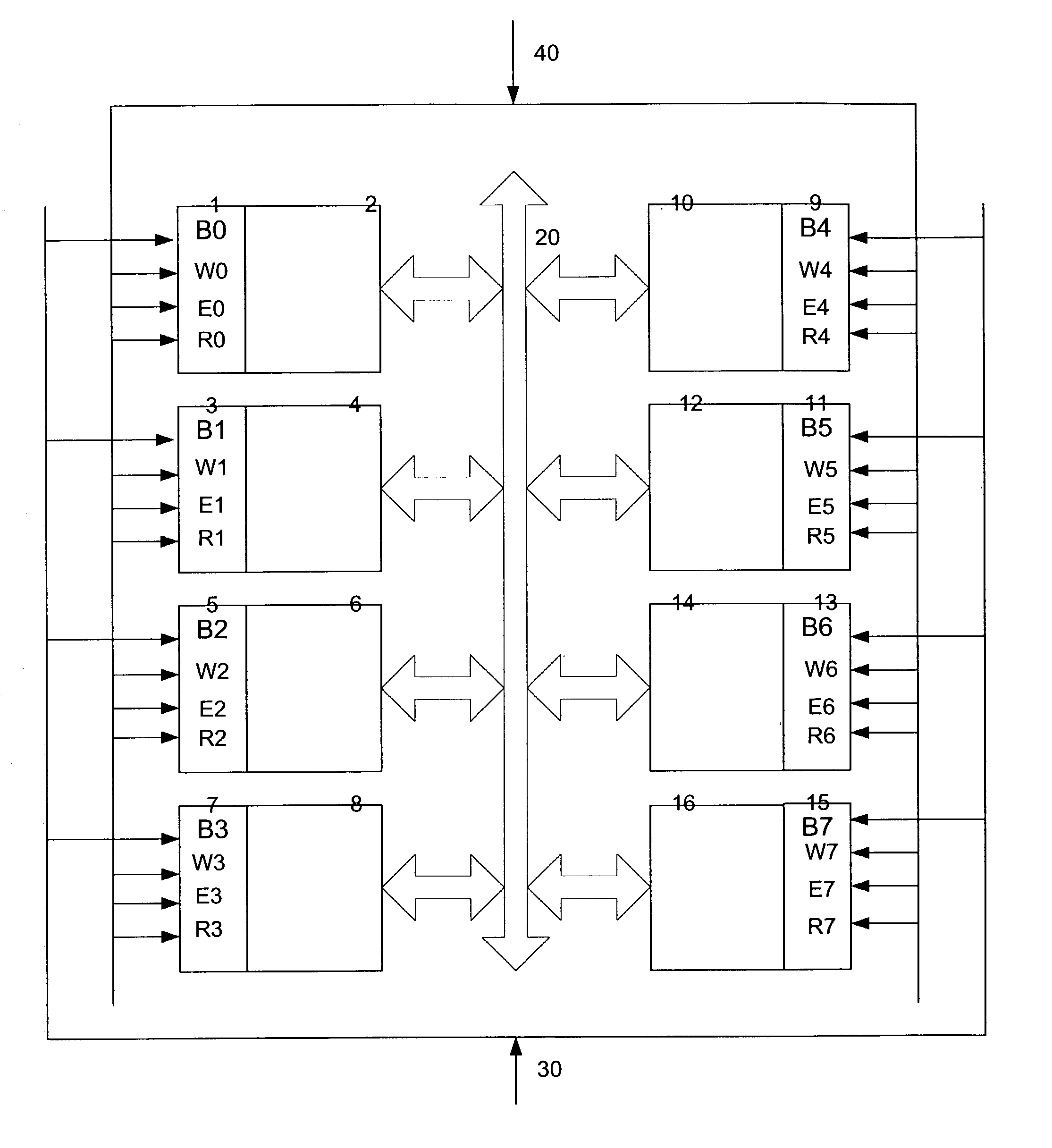
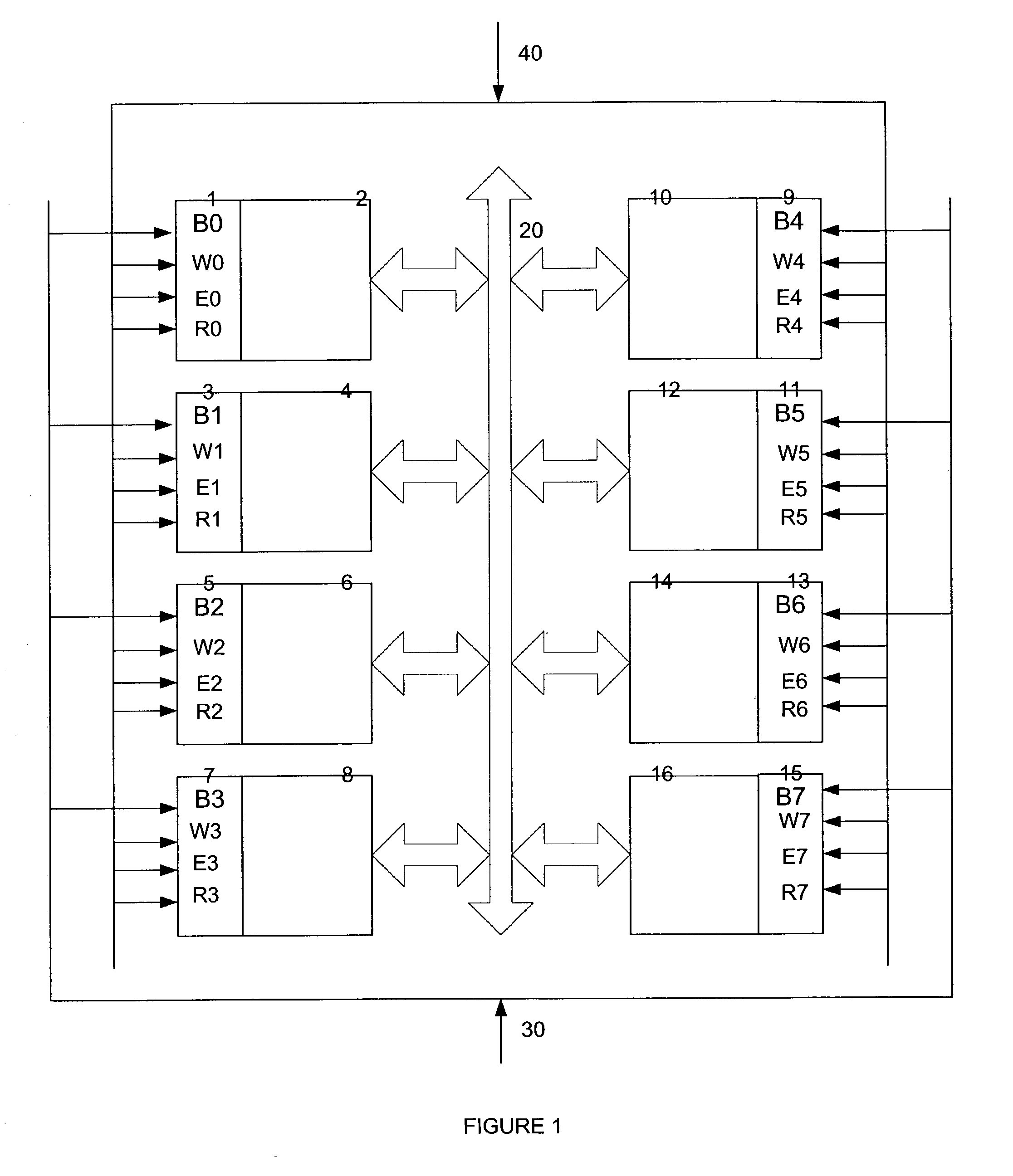
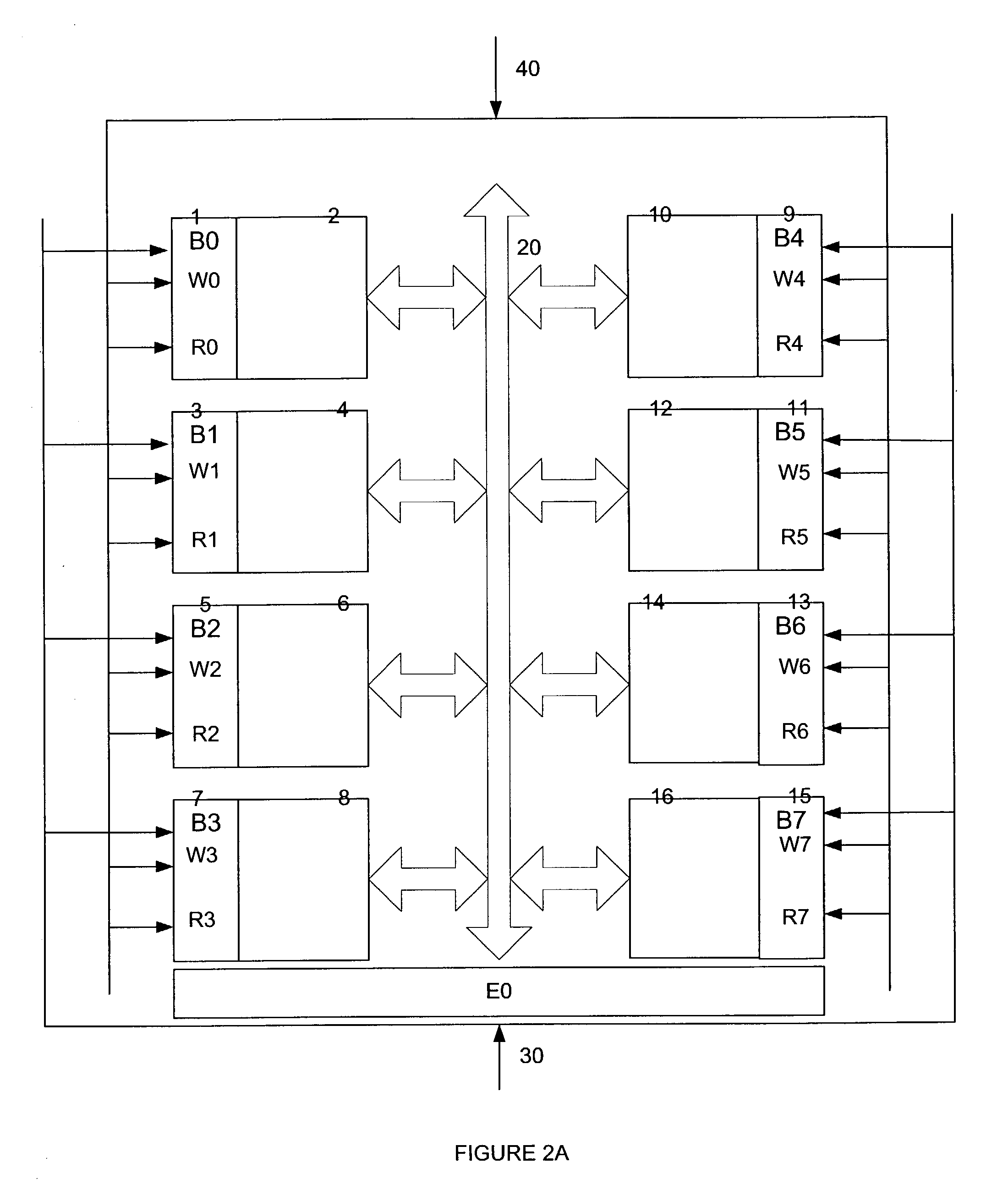
[0019]One possible approach to improve performance of a memory is to allow more than one operation to be performed on it at a time by dividing the memory into multiple independently addressable banks. By duplicating read, write, and erase circuits, any of these operations can be performed in parallel on multiple banks.

[0020]Write and erase circuitry generates large voltages, and thus the circuits require substantial area in the substrate. Until now, duplication of such circuits hasn't been designed into nonvolatile memory fabricated on a die in storage devices. (Integrated circuits are fabricated in or on a wafer. The wafer is then diced into discrete pieces, called die, which are then packaged, possibly along with other die, to be used in electronic devices.) The monocrystalline silicon substrate used in most semiconductor devices is expensive, and duplicating write and erase circuits requires using valuable substrate area, which, for nonvolatile memory on a die in storage devices,...


PUM


Abstract

A nonvolatile multibank memory on a die with multiple read, write, and erase circuits, allowing more than one bank to be read, written, erased, or tested independently. Such a multibank memory arrangement is used advantageously in a monolithic three dimensional memory formed above a substrate, leaving unused substrate area available in which the additional circuitry and related cache memory can be formed.

Description

BACKGROUND OF THE INVENTION[0001]Nonvolatile memories are commonly either rewriteable devices, such as charge-storage devices, or one-time programmable devices, such as antifuse devices. Charge storage devices are usually programmed using Fowler-Nordheim tunneling or channel hot electron injection, while programming of antifuse devices requires applying the large voltage required to blow an antifuse. These programming mechanisms are slow and do not become faster as memories shrink, meaning that, as a rule, nonvolatile memories are slower to access than volatile memories. Monolithic three dimensional memories like the ones described in Johnson et al., U.S. Pat. No. 6,034,882, Knall et al., U.S. Pat. No. 6,420,215; and Lee et al., U.S. patent application Ser. No. 09 / 927,648, filed Aug. 13, 2001, because of the extra distance data must travel to reach upper levels of memory, are slower still.[0002]There is a need, therefore, to improve the access time of nonvolatile memories.SUMMARY OF...

Claims


Application Information

Patent Timeline
IPC IPC(8): G11C16/06G11C7/00G11C16/10G11C7/22G11C29/04G11C29/26G11C16/08
CPCG11C7/22G11C16/10G11C29/26G11C16/08G11C2216/20G11C2216/22G11C2216/24G11C2216/26
Inventor FASOLI, LUCA G.SCHEUERLEIN, ROY E.
Owner SANDISK TECH LLC
Why Eureka
Try Eureka