Device transfer techniques for thin film optoelectronic devices

a technology of optoelectronic devices and device transfer techniques, which is applied in the field of fabric and optoelectronic devices, can solve the problems of substantial cost, significant impediment to successful commercialization, and the inability of the pet to withstand the temperature required for many desired thin film process steps

Inactive Publication Date: 2005-11-22
AERIS CAPITAL SUSTAINABLE IP
View PDF2 Cites 70 Cited by
  • Summary
  • Abstract
  • Description
  • Claims
  • Application Information

AI Technical Summary

Problems solved by technology

On the other hand, PET cannot withstand temperatures such as are required for many desired thin film process steps, especially those used in the manufacture of CIGS (CuInGaSe2) solar cells, which must be processed at 400–500° C. for times in the range of ½ to 1 hour or more.
This is a very substantial cost, and represents a significant impediment to successful commercialization.
Polyimides also have some undesirable properties when used at these temperatures; although they do not decompose, the thermal expansion induces stresses that may be problematic for film adhesion, and water absorption and outgassing in vacuum is an issue.
Thin metal foils eliminate concerns about thermal stability or mechanical deformation, but they have other problems.
Such foils are not sufficiently smooth as received from commercial sources, and must be polished by means which are not well developed and which add cost.
Metals are also more expensive than desired.
Unfortunately, these prior art processes suffer from several disadvantages.
If the metal has to be removed by etching, there is nothing to be gained from the cost viewpoint compared to leaving it in place.
In the case of Rudmann, et al., the glass substrate can be reused, but the removal of the sacrificial layer requires etching of a very thin layer from the side over a large area, which makes it undesirably slow.

Method used


Image

  • Device transfer techniques for thin film optoelectronic devices
  • Device transfer techniques for thin film optoelectronic devices
  • Device transfer techniques for thin film optoelectronic devices

Examples


Embodiment Construction

[0012]Although the following detailed description contains many specific details for the purposes of illustration, anyone of ordinary skill in the art will appreciate that many variations and alterations to the following details are within the scope of the invention. Accordingly, the exemplary embodiments of the invention described below are set forth without any loss of generality to, and without imposing limitations upon, the claimed invention.

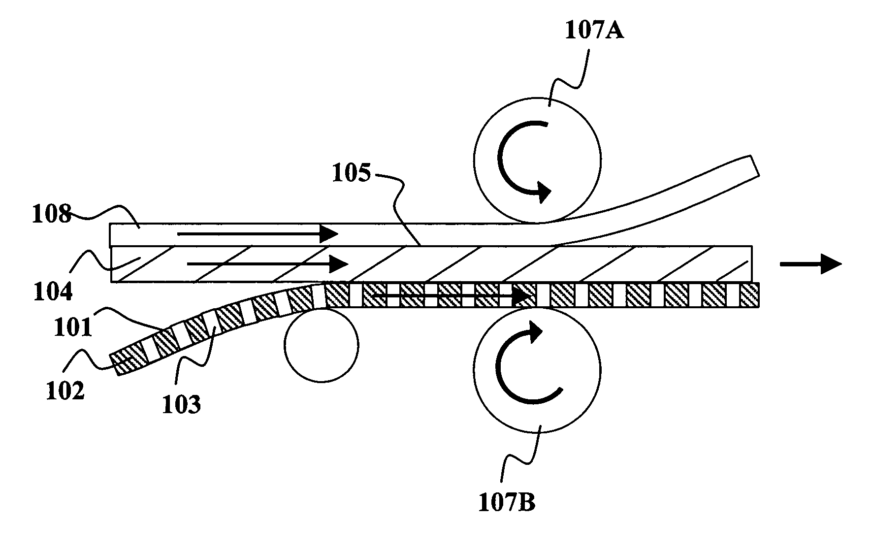
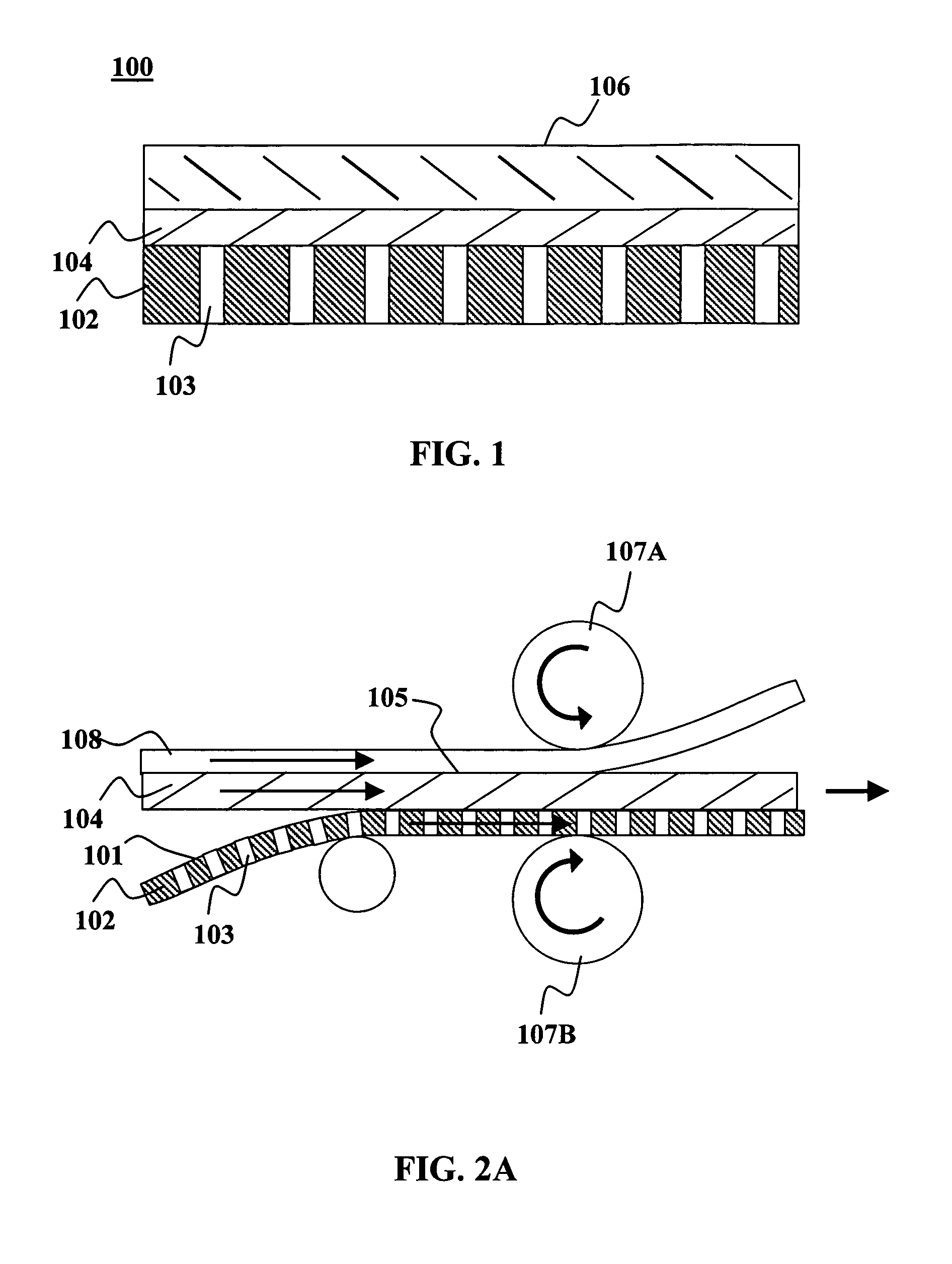
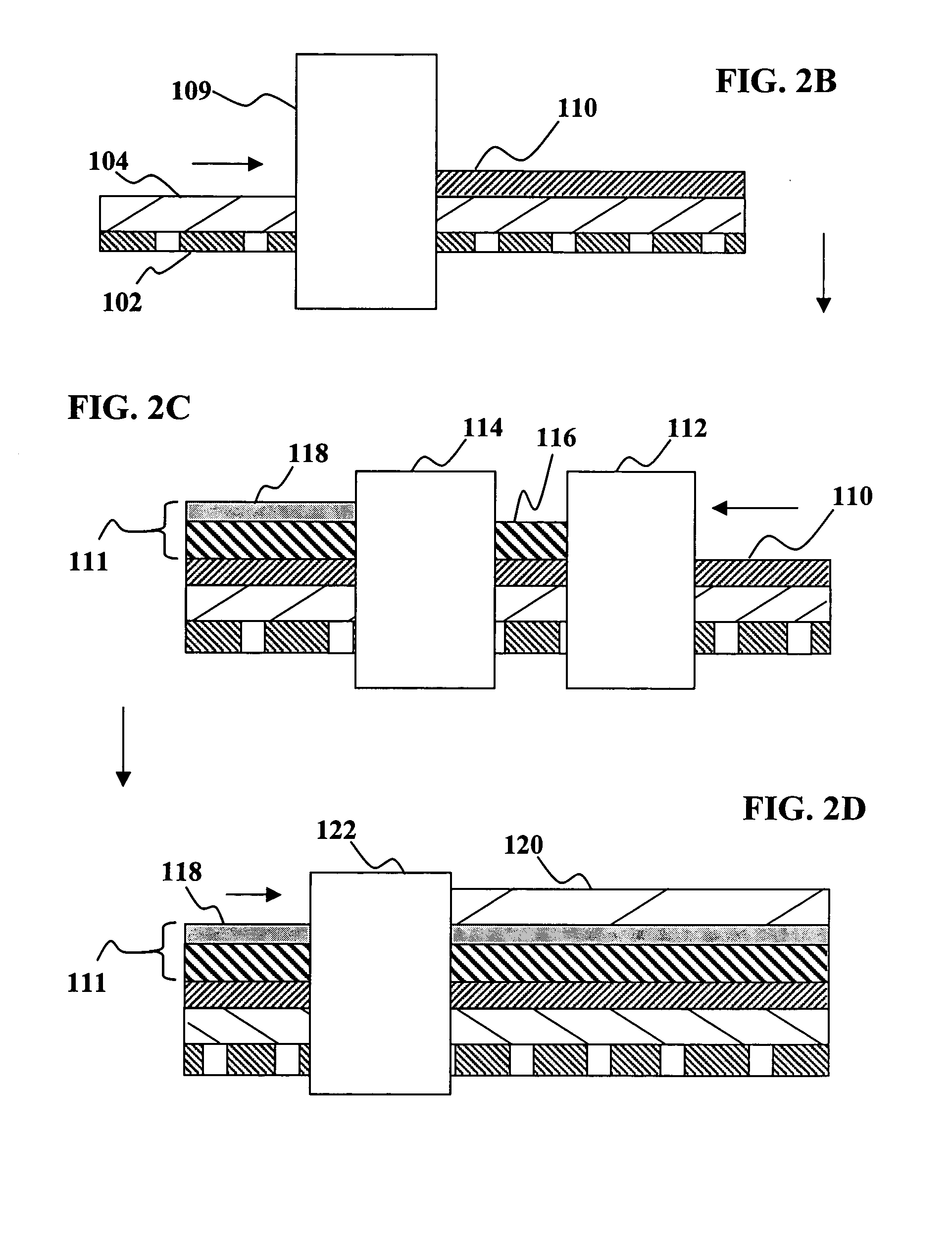
[0013]According to embodiments of the present invention, optoelectronic devices may be fabricated on a target substrate, which is optimized for the fabrication conditions, and then transferring them to a second substrate, which is optimized for the final product (including cost). By way of example, mostly likely the second substrate would be some other inexpensive but rugged industrial polymer, such as polyethylene terephthalate (PET). In embodiments of this invention a sacrificial layer is attached to a porous target substrate, and the devi...


PUM

PropertyMeasurementUnit
thicknessaaaaaaaaaa
thicknessaaaaaaaaaa
temperaturesaaaaaaaaaa

Abstract

A method for fabricating optoelectronic devices is disclosed. A sacrificial layer is deposited, formed or attached to a target substrate having a plurality of through holes. One or more device layers are formed on the sacrificial layer and the sacrificial layer is exposed to an etchant through the holes in the target substrate to detach the target substrate from the sacrificial layer without destroying the target substrate.

Description

FIELD OF THE INVENTION[0001]Embodiments of the present invention are directed to fabrication of optoelectronic devices and more specifically to fabricating optoelectronic devices on a reusable substrate.BACKGROUND OF THE INVENTION[0002]Optoelectronic devices interact with radiation and electric current. The interaction can be photoelectric where the device converts incident radiant energy (e.g., in the form of photons) into electrical energy. Alternatively Optoelectronic devices often tend to be high voltage and low current devices. Currently many optoelectronic devices, e.g., thin-film photovoltaic (PV) cells and organic light-emitting diodes (OLEDs) are made by depositing patterns of material on a substrate to form the various device layers, e.g., a bottom electrode, an active layer stack and a top electrode (plus auxiliary layers), of individual devices. In order to reduce the cost of thin film optoelectronic devices, such as solar cells, the use of inexpensive substrate material...

Claims


Application Information

Patent Timeline
Patent Type & Authority Patents(United States)
IPC IPC(8): H01L21/00
CPCH01L27/14683Y10S438/957
Inventor SHEATS, JAMES R.
Owner AERIS CAPITAL SUSTAINABLE IP
Why Eureka
Try Eureka