Multiple-chip probe and universal tester contact assemblage

a technology of probe needle and contact assemblage, which is applied in the direction of instrumentation, semiconductor/solid-state device testing/measurement, measurement devices, etc., can solve the problems of difficult manufacturing of the pitch of the probe needle and the angle of the projection of the probe needle, and the inability to achieve the close spacing necessary for testing some chips with conventional needle contacts, etc., to achieve the effect of reducing the time required for testing a wafer

Inactive Publication Date: 2005-11-29
TEXAS INSTR INC
View PDF3 Cites 48 Cited by
  • Summary
  • Abstract
  • Description
  • Claims
  • Application Information

AI Technical Summary

Benefits of technology

[0011]It is an object of the current invention to provide a wafer probe card assembly for testing one or more integrated circuits simultaneously, thereby significantly decreasing the time required to test a wafer.

Problems solved by technology

This is accomplished by bending the needles after they are mounted on the probe card, which is laborious, time consuming, and expensive.
However, the close spacing necessary for testing some chips cannot be achieved with conventional needle contacts.
The tight pitch of probe needles and the angles of their projection are extremely difficult to manufacture, and in turn insures a high cost.
Further, maintenance of such cards adds significantly to the cycle time of testing.
Photolithographic definition of the leads adds cost to the testing procedure, not only as a result of the initial cost and multiple steps involved, but also because new artwork and masks are required for each new device and / or change, thus adding to cycle time for production.
The issue of uniform contact, as well as alignment is aggravated by thermal expansion of the membrane because very often the chip generates a significant amount of heat during the testing procedure.
Further, with multiple touch downs and heat, probe tips become oxidized, and may require cleaning or replacement, thus adding to the test time.
However, the biggest wafer testing issue may be that of long test time.
Testing complexity, and the time required varies with the circuitry, but the alignment and positioning time may equal or exceed that of the testing itself.
Further, the size of semiconductor wafers has increased, and the geometry of circuitry has decreased, resulting in an increase in the number of chips per wafer.
Consequently, test time resulting in product delivery delays, as well as the cost associated with expensive tester utilization has become a very significant issue to the industry.

Method used


Image

  • Multiple-chip probe and universal tester contact assemblage
  • Multiple-chip probe and universal tester contact assemblage
  • Multiple-chip probe and universal tester contact assemblage

Examples


Embodiment Construction

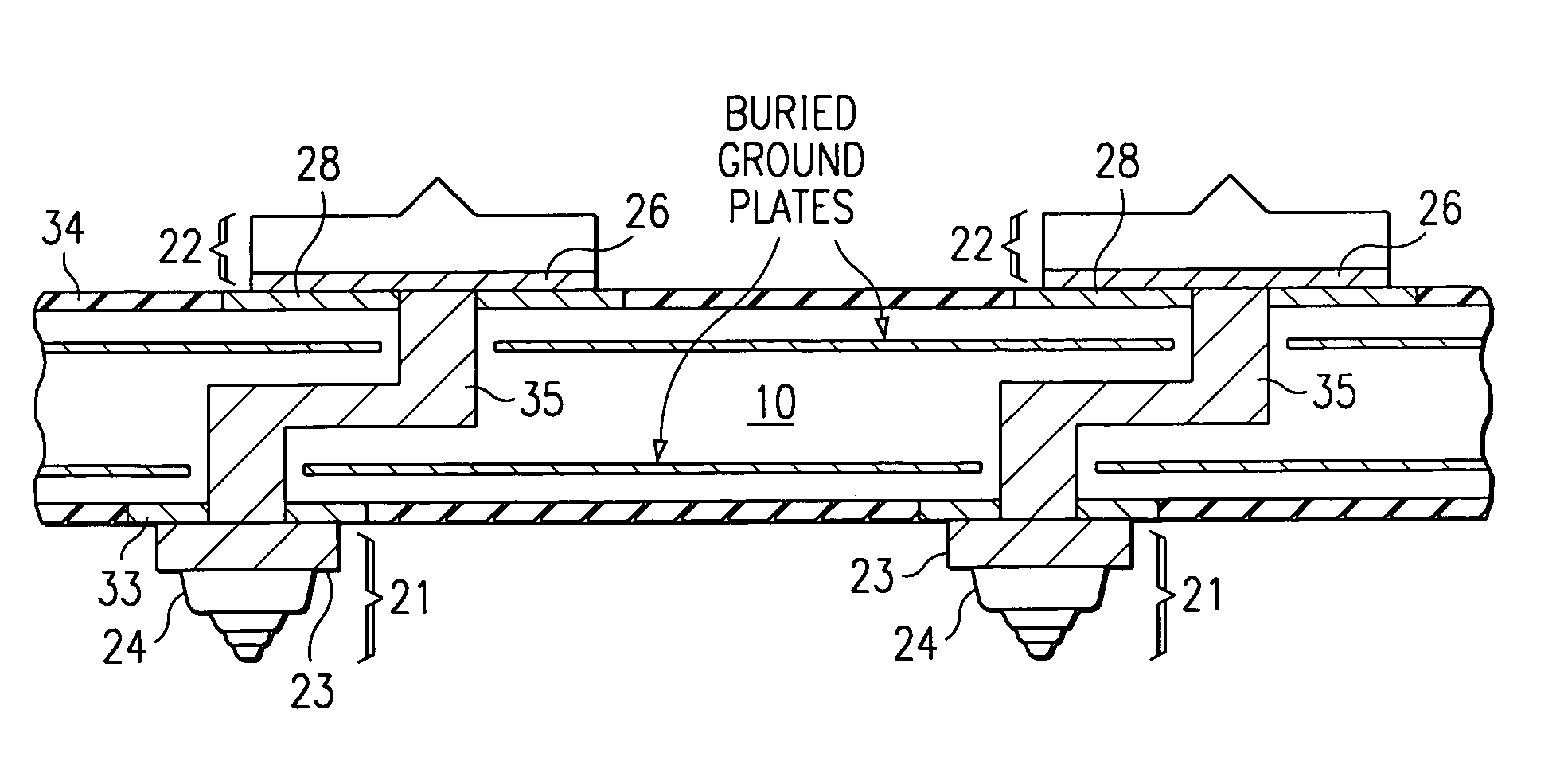
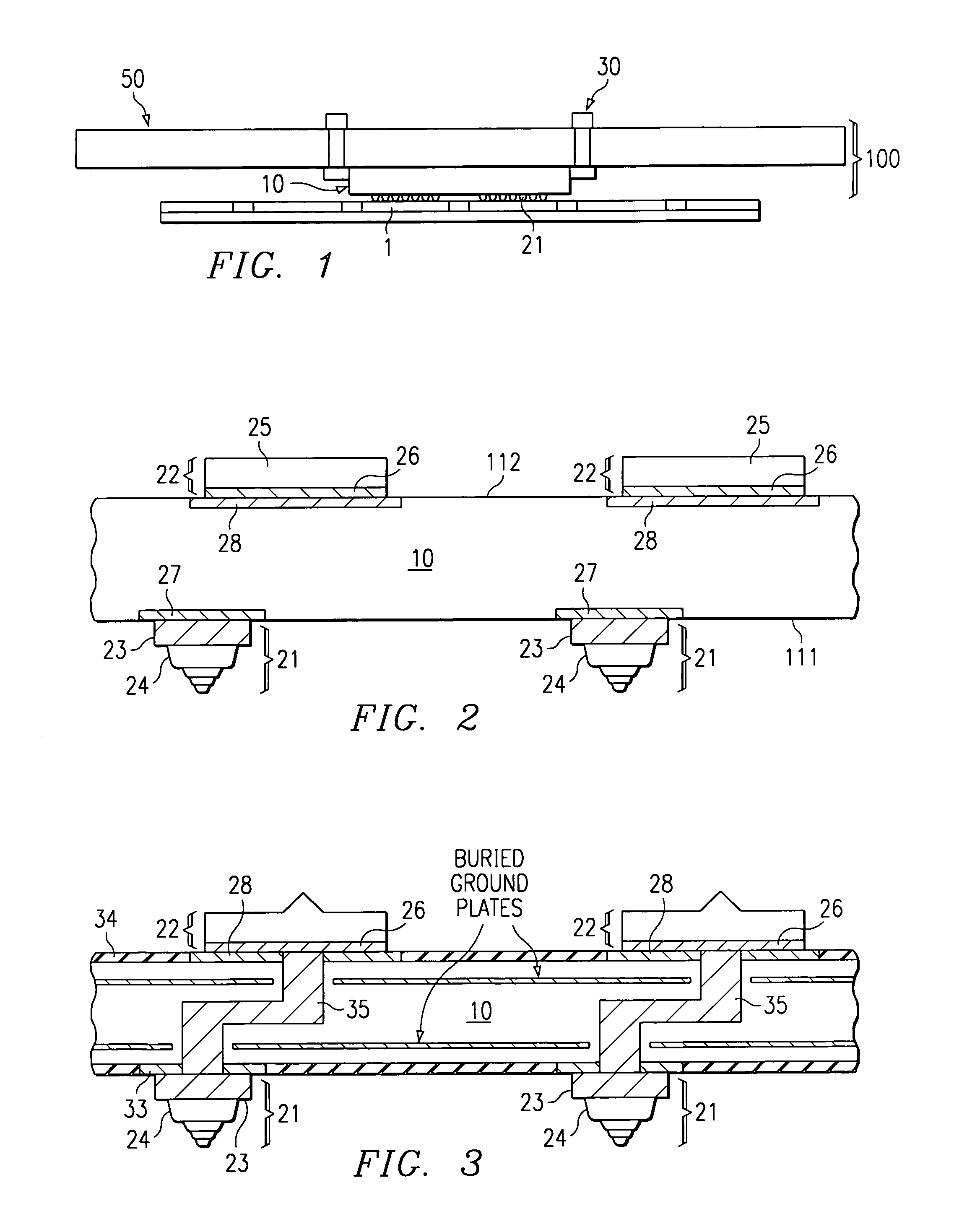
[0032]FIG. 1 is a multiple-chip probe assemblage 100 in accordance with the present invention. The assemblage 100 includes an interposer 10 having contact elements 21 for testing two (2) or more integrated circuit chips on a semiconductor wafer 1, a probe card 50 having universal or standardized contacts, and a means 30 to secure the interposer 10 to the probe card 50. The multiple-chip probe assemblage 100 is suitable for wafer testing at elevated temperatures. During testing of the chip sites on a wafer 1, the multiple-chip probe assemblage provides a means for contacting the input / output pads on the chips, and connecting with corresponding pads on a probe card 50 attached to a testing apparatus (not shown). The interposer of the multiple-chip probe assemblage minimizes adverse effects of thermal coefficient of expansion mismatches.

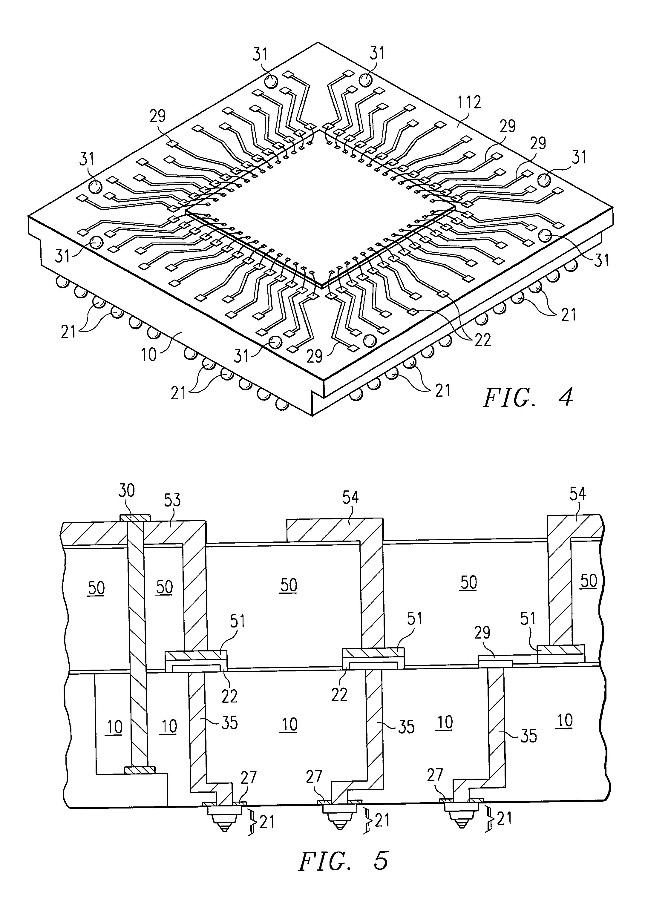
[0033]FIG. 2 provides a more detailed view of the interposer having contact elements on both of the major surfaces. A plurality of chip contact element...


PUM


Abstract

A probe card assemblage for simultaneously testing one or more integrated circuit chips including an interposer having on one surface a plurality of protruding contact elements for electrically contacting one or more chips of a wafer positioned atop a layer of compliant material, and arrayed in a pattern corresponding to a chip pads, a series of conductive vias through the electrically insulating interposer which connect the chip contact elements with an arrangement of leads terminating in a universal arrangement of connectors on the second surface, and a probe card with connectors mating to those on the interposer. The connectors on the interposer is secured are secured to those on the probe card, thereby providing a vertical probe assemblage which makes use of ultrasonic energy to minimize scrub or over travel. The universal probe card is specific to a tester configuration and common to a family of circuits to be tested.

Description

[0001]This application claims the benefit of Provisional Application No. 60 / 228,070, filed Aug. 24, 2000.FIELD OF THE INVENTION[0002]This invention relates to the testing of integrated circuits, and more particularly to a probe card apparatus for simultaneously testing multiple integrated circuit chips.DESCRIPTION OF PRIOR ART[0003]Integrated circuits (ICs) are formed as multiple, identical, discrete chips on a semiconductor crystal wafer. Each of the integrated circuit chips is usually tested to determine whether or not it functions as intended prior to cutting the semiconductor wafer into individual chips. Typically, the chips are tested by computer operated test apparatus that exercises the circuits on the chips, using a testing process commonly referred to as multiprobe testing.[0004]Conventional multiprobe testing employs a probe card which includes a plurality of electrical leads terminating in needles, which in turn make contact with input / output contacts of the various circu...

Claims


Application Information

Patent Timeline
Patent Type & Authority Patents(United States)
IPC IPC(8): G01R31/26G01R1/06G01R1/073H01L21/66
CPCG01R1/07378G01R1/07314
Inventor RINCON, REYNALDO M.ARNOLD, RICHARD W.
Owner TEXAS INSTR INC
Why Eureka
Try Eureka