

Liquid crystal display device, display device and manufacturing method thereof
a liquid crystal display device and display device technology, applied in non-linear optics, instruments, optics, etc., can solve the problems of difficult rapid driving of liquid crystal display devices, inability to feed required charges, and remarkable increase in voltage drop, so as to reduce the resistance of feeding electrodes, and accelerate the effect of driving
- Summary
- Abstract
- Description
- Claims
- Application Information
AI Technical Summary
Benefits of technology
Problems solved by technology
Method used
Image

Examples
first embodiment
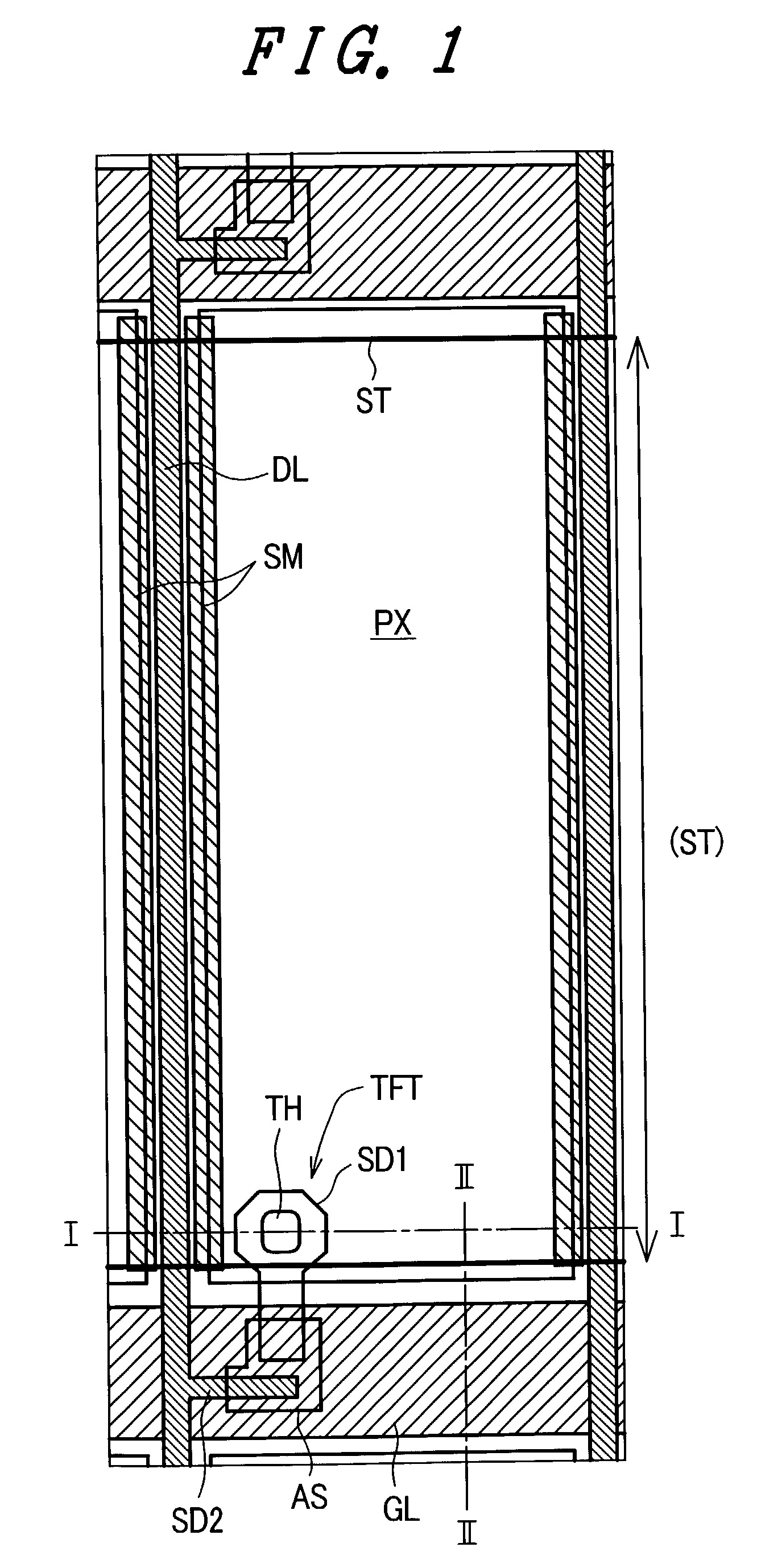
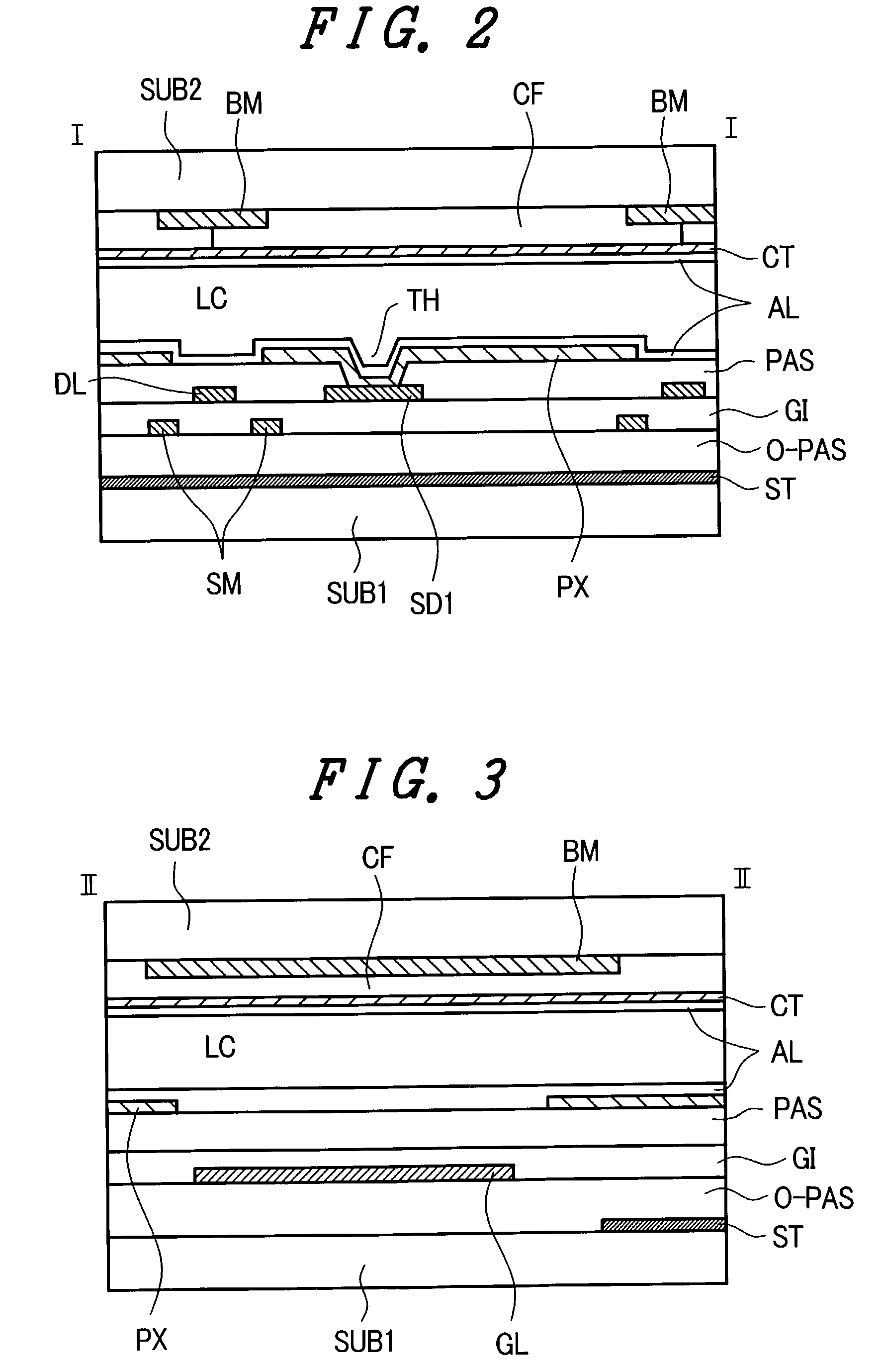
[0305]FIG. 1 is a plan view of the vicinity of one pixel of a vertical field type liquid crystal display device for schematically explaining the pixel constitution of the present invention. In the drawings, reference symbol PX indicates a pixel electrode, DL indicates drain lines (video signal lines or data lines), GL indicates gate lines (scanning lines), SM indicates a light shielding film (metal shield) which performs light shielding between the pixel electrode and the drain line, ST indicates a reference electrode layer (also referred to as a conductive layer), SD1 indicates a source electrode, SD2 indicates a drain electrode, AS indicates a semiconductor layer, and TH indicates a through hole. Here, the above-mentioned gate lines, drain lines and respective electrodes are referred to as electrode layers when they are explained in conjunction with cross sections.
[0306]FIG. 2 is a cross-sectional view taken along a line I—I in FIG. 1 and FIG. 3 is also a cross-sectional view take...
second embodiment
[0317]FIG. 4 is a plan view of the vicinity of one pixel of a vertical field type liquid crystal display device for schematically explaining the pixel constitution of the present invention, FIG. 5 is a cross-sectional view taken along a line I—I in FIG. 4, and FIG. 6 is a cross-sectional view taken along a line II—II in FIG. 4. Reference symbols in the drawings which are equal to those of the previous embodiment indicate identical functioning portions.
[0318]In this embodiment, the reference electrode layer ST has a region which includes regions where the gate line layer GL, the drain line DL and the pixel electrode layer PX of the first substrate SUB1 are formed. The holding capacity is formed between the pixel electrode layer PX and the reference electrode layer ST. According to this embodiment, since the reference electrode layer ST is formed below the gate line layer GL, it is desirable to set the thickness of the organic insulation layer O-PAS to equal to or more than 1 μm, for ...
third embodiment
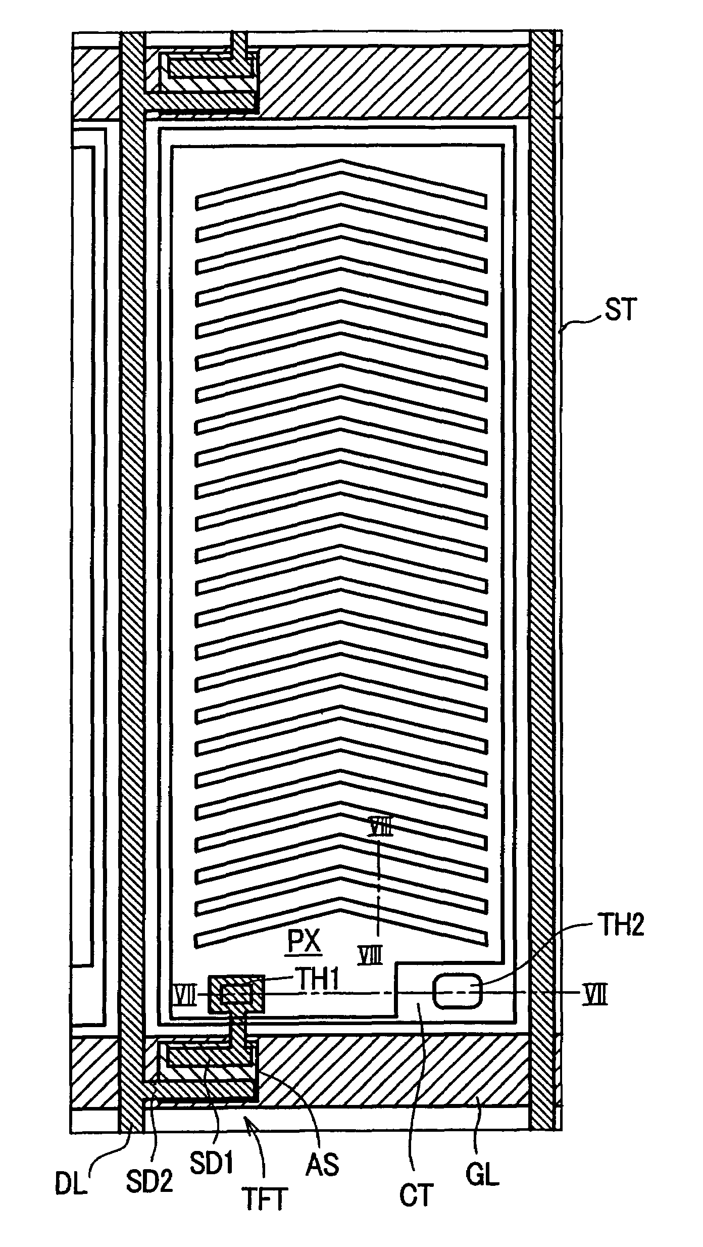
[0320]FIG. 7 is a plan view of the vicinity of one pixel of a vertical field type liquid crystal display device for schematically explaining the pixel constitution of the present invention and FIG. 8 is a cross-sectional view taken along a line I—I in FIG. 7. Reference symbols in the drawings which are equal to those of the previous embodiments indicate identical functioning portions. With respect to the pixel forming layer, over the organic insulation layer O-PAS, the gate line layer GL, the gate insulation layer GI, the drain line layer DL, the thin film transistor TFT, the passivation layer PAS and the pixel electrode PX are formed in this order. The whole or a portion of the pixel electrode PX in the pixel region penetrates the passivation layer PAS and is brought into contact with the gate insulation layer GI.
[0321]Due to such a constitution of this embodiment, in addition to the advantageous effects obtained by respective embodiments, the storage capacity formed between the re...
PUM
| Property | Measurement | Unit |
|---|---|---|
| thickness | aaaaa | aaaaa |
| size | aaaaa | aaaaa |
| transparent | aaaaa | aaaaa |
Abstract
Description
Claims
Application Information