Method and apparatus for improving stability of a 6T CMOS SRAM cell

a sram cell and stability technology, applied in the field of semiconductor integrated circuit design and manufacturing, can solve the problems of limiting the total transistor count of conventional 6t sram-dominated high performance, reducing the snm caused by increasingly smaller transistor geometries, and increasing the cell ratio corresponding to an area penalty in the form of increasing cell siz

Inactive Publication Date: 2005-11-29
TAHOE RES LTD
View PDF7 Cites 83 Cited by
  • Summary
  • Abstract
  • Description
  • Claims
  • Application Information

AI Technical Summary

Problems solved by technology

This reduction in SNM caused by increasingly smaller transistor geometries is undesirable.
This limits the total transistor count for conventional 6T SRAM-dominated high performance CMOS ASICs and microprocessors due to die size and cost constraints.
However, increasing the cell ratio corresponds to an area penalty in the form of increasing cell size.

Method used


Image

  • Method and apparatus for improving stability of a 6T CMOS SRAM cell
  • Method and apparatus for improving stability of a 6T CMOS SRAM cell
  • Method and apparatus for improving stability of a 6T CMOS SRAM cell

Examples


Embodiment Construction

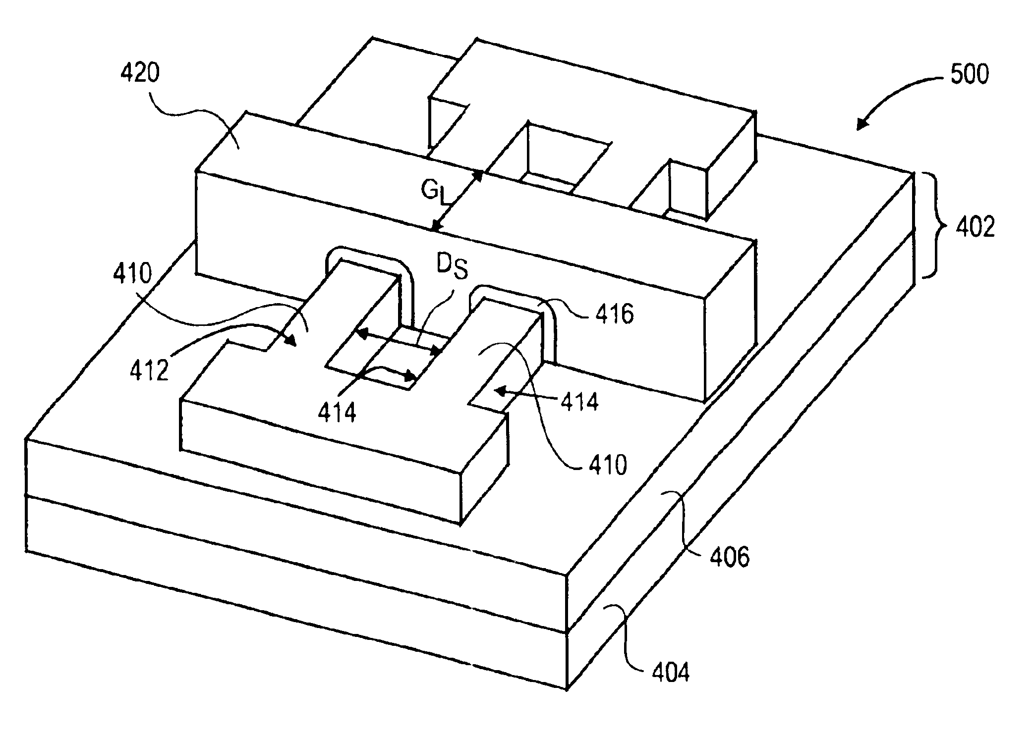
[0021]The present invention is a 6T CMOS SRAM cell using non-planar tri-gate transistors, and its method of fabrication. In the following description, numerous specific details are set forth in order to provide a thorough understanding of the present invention. In other instances, well-known semiconductor process and manufacturing techniques have not been described in particular detail in order to not unnecessarily obscure the present invention.

[0022]The present invention takes advantage of the higher drive current performance of non-planar tri-gate transistors to improve the stability of the 6T CMOS SRAM cell, thus enabling lower supply voltage operation and reduced cell layout sizes. Tri-gate transistors in multiple fin configurations can deliver more drive current for a given layout width than a planar transistor.

[0023]FIG. 4 illustrates a cross section of a typical single fin tri-gate transistor 400. A single fin tri-gate transistor is a tri-gate transistor having a single semic...


PUM


Abstract

The present invention is a CMOS SRAM cell comprising two access devices, each access device comprised of a tri-gate transistor having a single fin; two pull-up devices, each pull-up device comprised of a tri-gate transistor having a single fin; and two pull-down devices, each pull-down device comprised of a tri-gate transistor having multiple fins. A method for manufacturing the CMOS SRAM cell, including the dual fin tri-gate transistor is also provided.

Description

BACKGROUND OF THE INVENTION[0001]1. Field of the Invention[0002]The present invention relates to the field of semiconductor integrated circuit design and manufacturing, and more specifically to a 6T CMOS SRAM cell using tri-gate fully depleted substrate transistors and its methods of fabrication.[0003]2. Discussion of Related Art[0004]As silicon technology continues to scale from one generation to the next, the impact of intrinsic threshold voltage (Vt) variations in minimum geometry size bulk planar transistors reduces the CMOS SRAM cell static noise margin (SNM). This reduction in SNM caused by increasingly smaller transistor geometries is undesirable. SNM is further reduced when Vcc is scaled to a lower voltage.[0005]Threshold voltage (Vt) variations in planar transistors arise mostly from the statistical fluctuation of the number and / or location of the dopant atoms in the depletion region of the transistors. The Vt variations pose barriers to the scaling of supply voltage, trans...

Claims


Application Information

Patent Timeline
Patent Type & Authority Patents(United States)
IPC IPC(8): G11C11/412H01L21/336H01L21/8244H01L27/11H01L29/423H01L29/786
CPCG11C11/412H01L21/845H01L27/11H01L27/1104H01L27/1211H01L29/42384H01L29/785H01L29/66795H01L29/7854H10B10/00H10B10/12H01L27/146
Inventor DATTA, SUMANDOYLE, BRIAN S.CHAU, ROBERT S.KAVALIEROS, JACKZHENG, BOHARELAND, SCOTT A.
Owner TAHOE RES LTD
Why Eureka
Try Eureka