Reducing tester channels for high pinout integrated circuits

a technology of integrated circuits and testers, applied in the direction of measurement devices, error detection/correction, instruments, etc., can solve the problems of threatening to overtake all other manufacturing costs, conventional testers that have a limited number of test channels, and limiting factors of conventional testers, etc., to prolong the life of ic testers, short test times, and low test costs

Inactive Publication Date: 2005-11-29
MONTEREY RES LLC
View PDF35 Cites 35 Cited by
  • Summary
  • Abstract
  • Description
  • Claims
  • Application Information

AI Technical Summary

Benefits of technology

[0005]The objects, features and advantages of the present invention include providing a method and/or architecture for an integrated circuit that may (i) optimize use of tester channels, (ii) operate with existing circuitry on tester boards, (iii) provide for reliable testing, (iv) provide for short test times as

Problems solved by technology

Test costs of integrated circuits (IC) are progressively threatening to overtake all other manufacturing costs.
IC makers are packing a far wider range of functions with large number of pins causing conventional IC testers that have a limited number of test channels to become obsolete.
Conventional testers bec

Method used


Image

  • Reducing tester channels for high pinout integrated circuits
  • Reducing tester channels for high pinout integrated circuits
  • Reducing tester channels for high pinout integrated circuits

Examples


Embodiment Construction

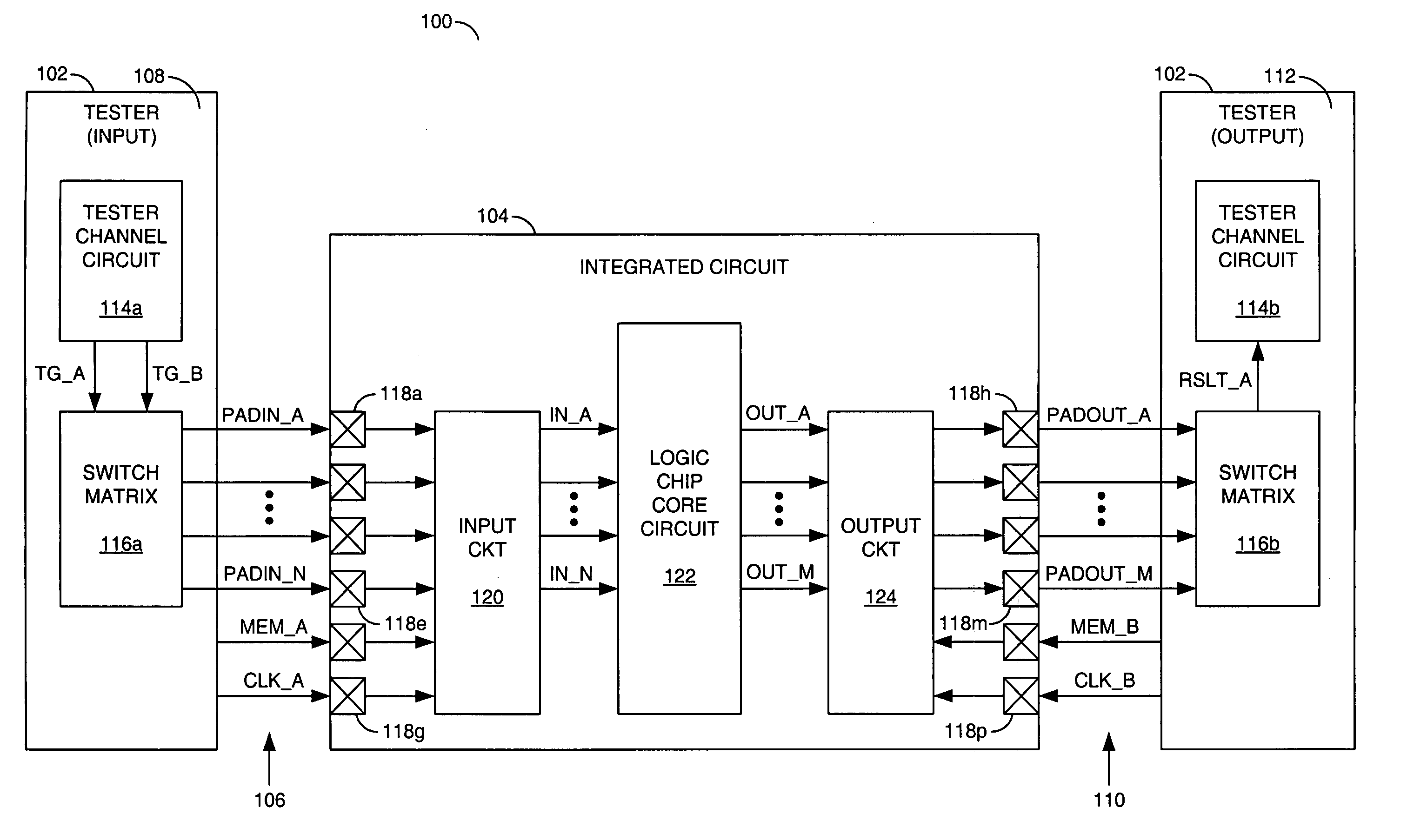
[0012]Referring to FIG. 1, a block diagram of a system 100 is shown in accordance with a preferred embodiment of the present invention. The system 100 generally comprises a tester 102 (shown in two places) and a device under test 104. The tester 102 may be an integrated circuit tester. The device under test 104 may be an integrated circuit (IC).

[0013]In one embodiment, the IC 104 may be implemented as a very large scale integration (VLSI) integrated circuit such as a programmable logic circuit, application specific integrated circuits, mixed signal devices, large gate array circuits or the like. In another embodiment, the IC 104 may be implemented as an ultra large scale integration (ULSI) integrated circuit. In still another embodiment, the IC 104 may be implemented as a system on a chip (SOC) integrated circuit. The IC 104 may be implemented as other types of circuits and / or systems to meet the design criteria of a particular application.

[0014]Multiple interfaces 106 may couple an...


PUM


Abstract

An integrated circuit generally comprising a plurality of input pads, an input circuit, and a core circuit. The input pads may be configured to receive a plurality of first input signals. The input circuit may be configured to generate a plurality of second input signals (i) equal to the first input signals while in an operational mode and (ii) responsive to a plurality of test vectors with timing generation determined by the first signals while in a test mode. The core circuit may be responsive to the second input signals.

Description

FIELD OF THE INVENTION[0001]The present invention relates to a method and / or architecture for integrated circuit testing generally and, more particularly, to a method and / or architecture for implementing high pinout digital integrated circuits having on-chip circuitry that supports external testers.BACKGROUND OF THE INVENTION[0002]Test costs of integrated circuits (IC) are progressively threatening to overtake all other manufacturing costs. IC makers are packing a far wider range of functions with large number of pins causing conventional IC testers that have a limited number of test channels to become obsolete. Current technology IC testers operate by classifying IC inputs into different categories, store test patterns in a tester memory buffer, and supply direct current (DC) levels for each of the IC inputs from dedicated tester channels. Appropriate sets of the DC levels are selected through board-level multiplexers for each IC pin. The levels are further controlled by a bit conf...

Claims


Application Information

Patent Timeline
IPC IPC(8): G01R31/317G01R31/319G06F11/00G06F11/263
CPCG01R31/3172G01R31/31926G01R31/31928G06F11/263
Inventor DEB, BISWA M.GUPTA, RAJAT
Owner MONTEREY RES LLC
Why Eureka
Try Eureka