Semiconductor device and method of manufacturing the same

a semiconductor and trench gate technology, applied in semiconductor devices, digital storage, instruments, etc., can solve the problems of deteriorating film quality unable to meet the voltage of gate insulating films, etc., and achieve the effect of suppressing the voltage of laminate films

Active Publication Date: 2005-12-13
DENSO CORP
View PDF11 Cites 6 Cited by
  • Summary
  • Abstract
  • Description
  • Claims
  • Application Information

AI Technical Summary

Benefits of technology

[0012]Furthermore, since the first silicon oxide film at the trench side is set to be larger than the film thickness of the second silicon oxide film at the polysilicon side, the rate of a boron-unpolluted area to the overall laminate film can be increased as compared with a case where the film thickness of the second silicon oxide film is set to

Problems solved by technology

Accordingly, the film quality of the gate insulating film is deteriorated, which may res

Method used


Image

  • Semiconductor device and method of manufacturing the same
  • Semiconductor device and method of manufacturing the same
  • Semiconductor device and method of manufacturing the same

Examples


first embodiment

(First Embodiment)

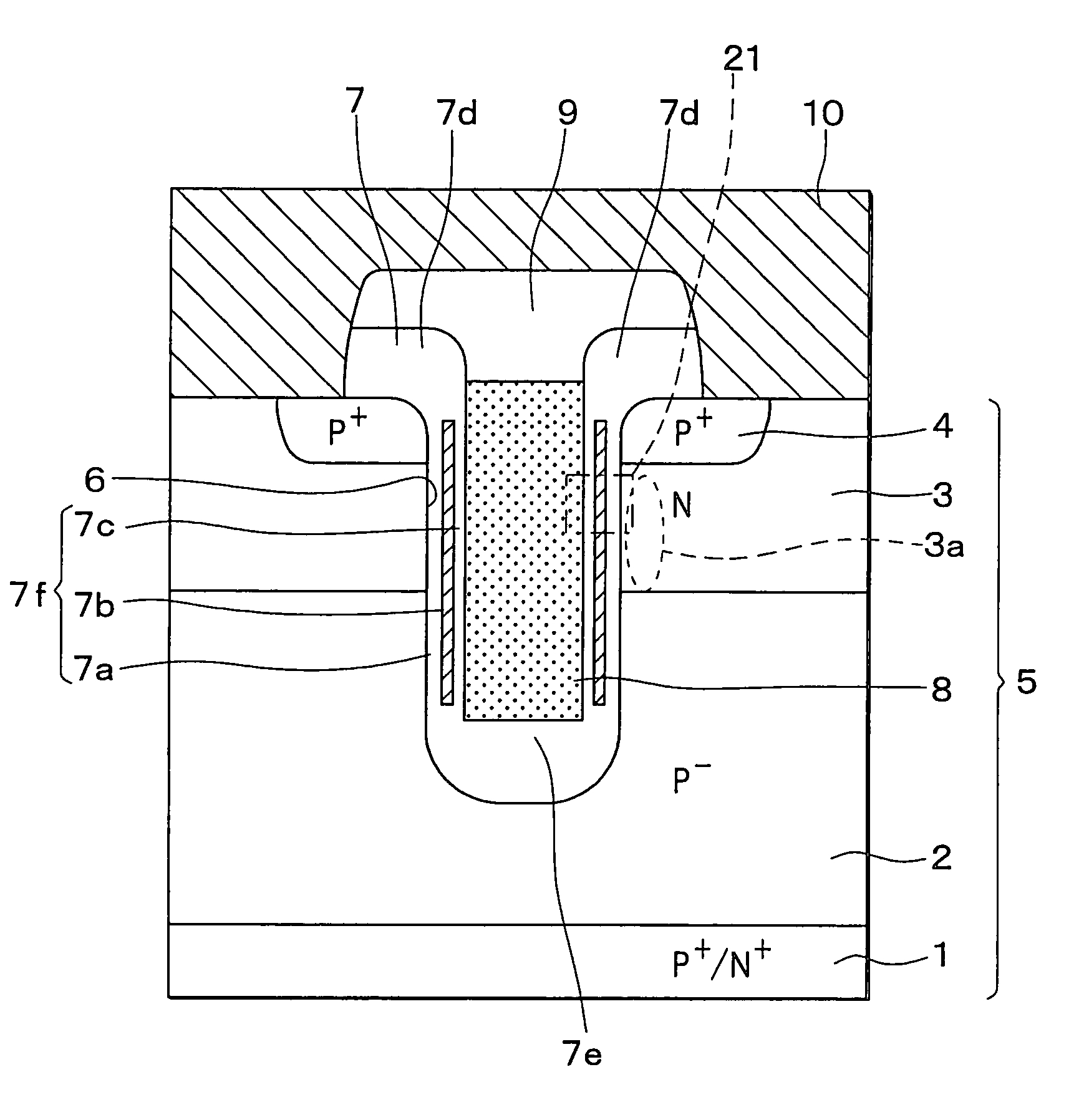
[0023]FIG. 1 is a cross-sectional view showing a semiconductor device implemented according to an embodiment of the present invention. This semiconductor device if for implementing a transistor having a trench-gate structure such as a power MOSFET, IGBT or the like. A preferred embodiment will be described with respect to a P-channel type transistor.

[0024]In FIG. 1, a P-type drift layer 2 is formed on a P+-type or N+-type silicon substrate 1, and an N-type layer 3 serving as a base region is formed on the drift layer 2. A P+-type layer 4 serving as a source region is formed in the N-type layer 3. A semiconductor substrate 5 comprises these elements.

[0025]Furthermore, a trench 6 is formed in one surface of the semiconductor substrate 5 so as to penetrate through the P+-type layer 4 and the N-type layer 3, and to reach the drift layer 2. Gate insulating film 7 is formed on the inner wall of the trench 6. A gate electrode 8 is further embedded through the gate insulat...

second embodiment

(Second Embodiment)

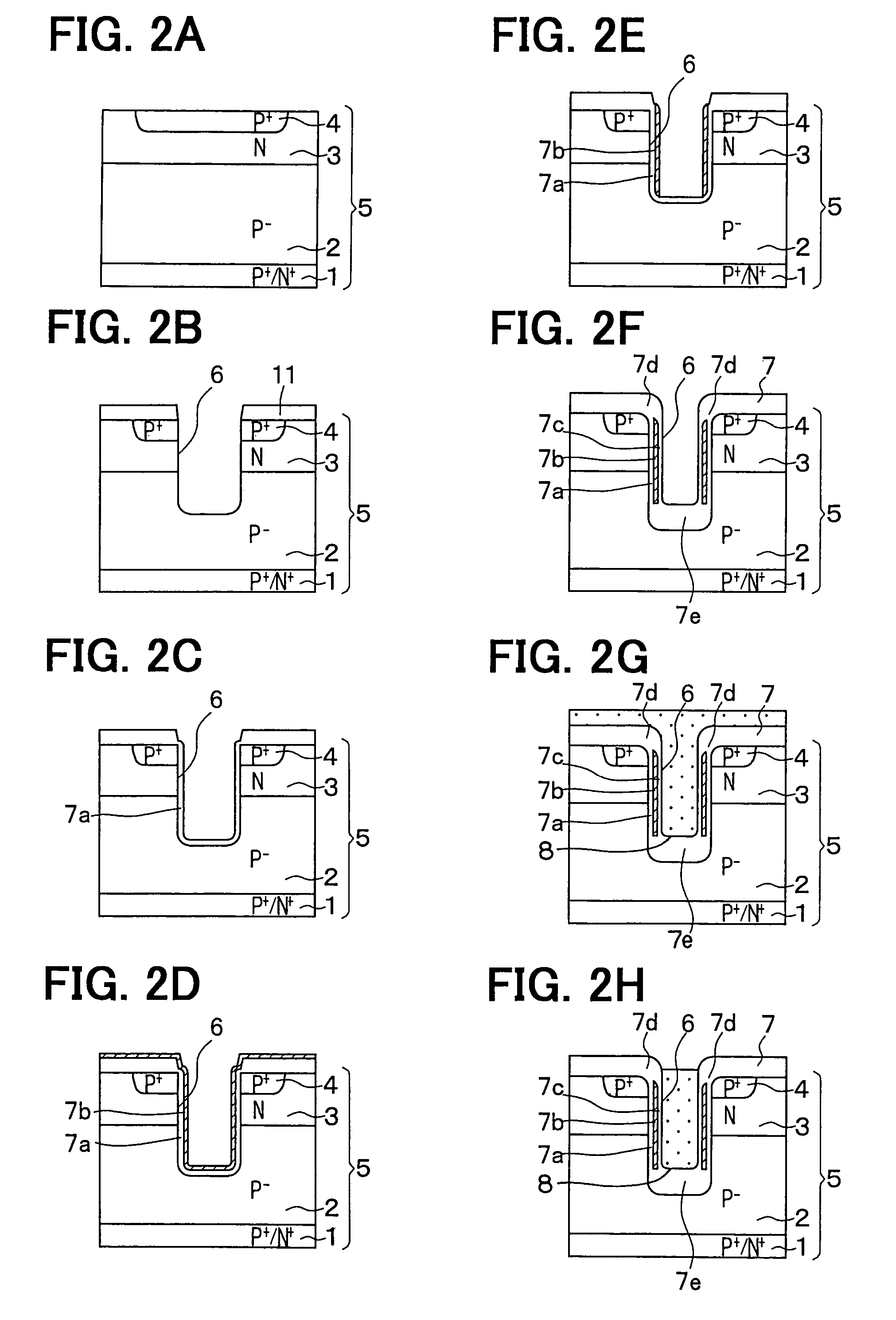
[0055]In the first embodiment as described above, according to the method of manufacturing the trench-gate type semiconductor device, the N-type layer 3 serving as the base region and the P+-type layer 4 serving as the source region are formed before the gate electrode 8 is formed. However, after the gate electrode 8 is formed, the N-type layer 3 and the P+-type layer 4 may be formed by the ion implantation and the thermal treatment to diffuse the impurities.

[0056]In this case, the manufacturing process is altered as follows. More particularly, the formation of the N-type layer 3 and the P+-type layer 4 is not carried out in the step of FIG. 2A out of FIGS. 2A to 2H, and in the step of FIG. 2H, the silicon oxide film 11 on the surface of the area for forming the N-type layer 3 and the P+-type layer 4 of the drift layer 2 is removed after the gate electrode is formed. Thereafter, the N-type layer 3 and the P+-type layer 4 are formed by the ion implantation and the ...


PUM


Abstract

In a semiconductor device having a trench-gate structure in which polysilicon doped with boron is embedded in a trench, insulating film formed on the inner wall of the trench comprises ONO film, and silicon nitride film constituting the ONO film is formed to such film thickness and film quality that boron can be suppressed from passing through the silicon nitride film. Silicon oxide film is formed so that a top oxide film is thin and a bottom oxide film is thick.

Description

CROSS REFERENCE TO RELATED APPLICATION[0001]This application is based upon, claims the benefit of priority of, and incorporates by reference the contents of Japanese Patent Application No. 2003-14466 filed on Jan. 23, 2003.BACKGROUND OF THE INVENTION[0002]1. Field of the Invention[0003]The present invention relates to a semiconductor device and a manufacturing method therefore and, more particularly, to a semiconductor device having a trench gate structure and a manufacturing method therefore.[0004]2. Description of the Related Art[0005]Semiconductor devices having a trench gate structure in which gate insulating film is formed on a side wall of a trench formed in one surface of a semiconductor substrate and in which a gate electrode is embedded in the trench are known.[0006]In some of the semiconductor devices as described above, the gate insulating film comprises laminate film formed of silicon oxide film, silicon nitride film and silicon oxide film, referred to as ONO (Oxide Nitr...

Claims


Application Information

Patent Timeline
IPC IPC(8): H01L21/28H01L21/331H01L21/336H01L29/423H01L29/51H01L29/739H01L29/78
CPCH01L21/28185H01L21/28194H01L29/513H01L29/518H01L29/66348H01L29/7397H01L29/7813H01L29/42368Y10S257/90
Inventor SHIGA, TOMOFUSAAOKI, TAKAAKIOKABE, YOSHIFUMI
Owner DENSO CORP
Why Eureka
Try Eureka