Methods and devices for eddy current PCB inspection

a technology of eddy current and inspection method, applied in the direction of magnetic property measurement, material magnetic variable, instruments, etc., can solve the problems of deteriorating the functionality affecting the inspection efficiency of the pcb, and affecting the inspection efficiency of the assembled pcb, so as to achieve the inspection of the pcb very quickly

Inactive Publication Date: 2005-12-13
BILIK YULI +2
View PDF22 Cites 25 Cited by
  • Summary
  • Abstract
  • Description
  • Claims
  • Application Information

AI Technical Summary

Benefits of technology

[0017]Another object of the invention is to achieve a sharp focus of the EM field flux on the PCB surface to be inspected, by placing an external magnetic field concentrator on the opposite side of the PCB to improve defects detection and eddy current image resolution.
[0032]Finally, the present invention discloses an EC system for non-contact, real time PCB inspection, based on the EC transducer and the method of PCB layers separation mentioned above. The system preferably includes two arrays of EC transducers that simultaneously and synchronously scan two respective PCBs, one known as a “good” workpiece and the other known as the “inspected” one. The system allows to inspect the PCB very quickly, even without a computerized aided manufacturing (CAM) database of PCB layer images (Gerber files), which are provided in general by a layout engineer.

Problems solved by technology

Although etching processes are precisely prepared and controlled, some defects may appear on a PCB.
Defects such as opens or shorts may immediately lead to rejection of the PCB, while micro-semi-cracks or filamentary shorts, poor cleanliness, or geometrical changes in the conducting paths may create hidden faults, which may deteriorate the functionality of the assembled PCB to the point of rendering it useless.
A manual visual method is limited in performance, labor-intensive and prone to human fatigue.
Both visual and laser methods have high optical resolution, but are limited in their ability to reveal narrow cracks or filament-type shorts and other invisible flaws, such as salt, residues left over from the etching process, or under-etching characterized by a series of random copper dots and partially conducting surfaces.
As mentioned by Finarov in U.S. Pat. No. 5,333,052, an optical inspection system becomes ineffective, generating many false alarms when the conductive surfaces suffer from colorization due to metal oxidation (which changes color and reflectivity).
However, laser-based optical inspection cannot be used to distinguish between two non-fluorescing materials, such as two metal layers, or to image a thin insulating film on a metal layer that does not fluoresce because of its composition or thinness.
A “flying probes” technique is very slow and of low effectiveness.
Along with the recent developments in high-density PCBs with extremely fine parts and wiring patterns, it has become difficult to correctly position test probes onto the areas to be inspected in the case of inspections using an in-circuit tester.
Moreover, when test probes are positioned on a high density PCB, the circuit board might be damaged due to disconnections induced in the wiring pattern, as mentioned by Kawaike et al in U.S. patent application Ser. No. 10 / 198,739.
Additional disadvantages of ECT include its incapability to localize the position of a defect, and its low ability to observe conducting path geometry violations.
These technologies require very expensive and complex equipment, also involving safety issues.
In general, thermal methods are characterized by low resolution and complex processing.
The main limitation of this system is its low resolution and the impossibility to reveal defects in the Z (depth) direction.
In other words, Soiferman's method cannot provide a high resolution 3-dimensional PCB pattern image.
The main limitation of Daalmans' method and system is the low inductivity of the coils, which requires the use of an excitation signal from a transmitter coil at very high frequencies.
This means that the EC penetration depth is very small, and that it is impossible to detect any defects inside the subsurface region.
This feature makes the method non-universal and labour-intensive.
Any defect in the conducting surface will disrupt the flow of induced current.
Kawaike's detection method has low resolution for distinguishing between faulty and good patterns, and cannot determine the type of defect and its lateral localization in the PCB.
Their technique is limited by the very small signal generated by the tangential component, which is very difficult to preserve in practice when high scanning velocities are used.
Another limitation of the tangential component measurement is the substantial difficulty in inspecting a multilayer PCB.
The main disadvantage of each of these methods is the requirement to use a wide range of driving frequencies to change the penetration depth.
Therefore, the resolution of the testing sensor becomes very critical.

Method used


Image

  • Methods and devices for eddy current PCB inspection
  • Methods and devices for eddy current PCB inspection
  • Methods and devices for eddy current PCB inspection

Examples


Embodiment Construction

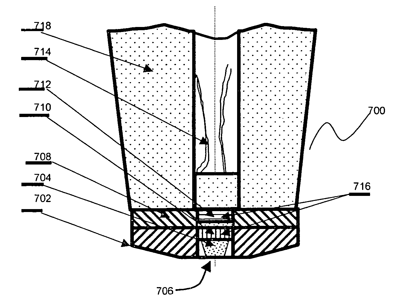
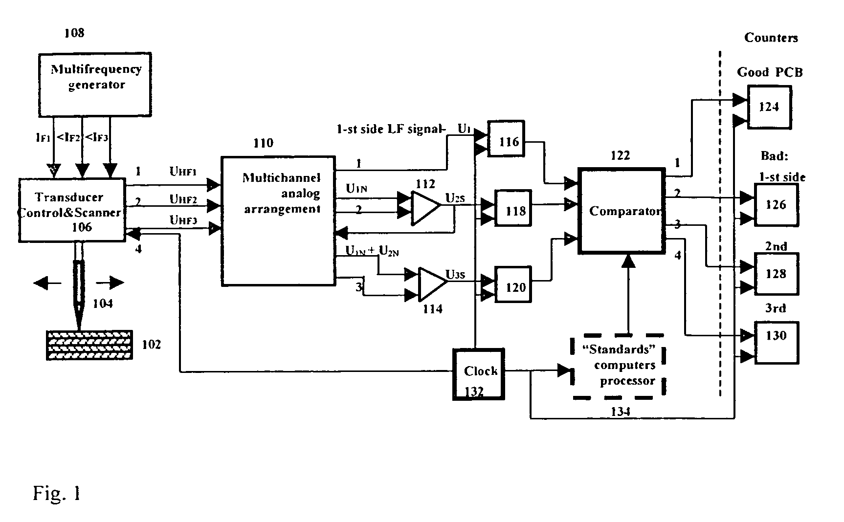
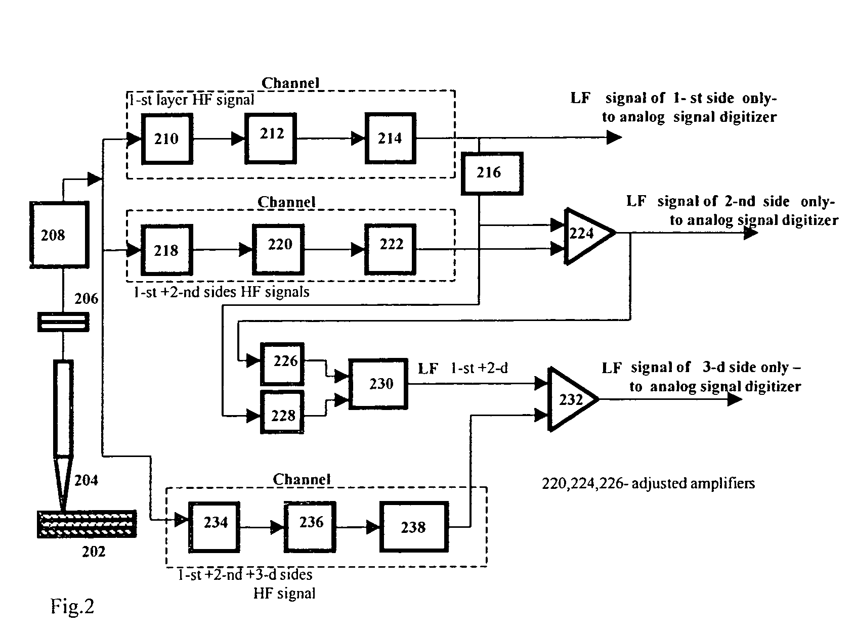
[0043]The present invention provides eddy current devices, systems and methods used to inspect single and multilayer PCBs, and to receive information from every PCB layer separately. The systems and methods include further data processing of the sensed information. The invention discloses a novel transducer having a ferrite core with preferably a sharp conical, pointed end, which provides a high EM field gradient in the small gap, typically 0.5–0.2 mm, between the transducer and the inspected PCB surface. In a preferred embodiment, a sharp focus of the electromagnetic field is obtained on the PCB surface by placing an external electromagnetic field concentrator on the opposite side of the PCB. A transducer with maximal resolution is obtained by choosing a correct value of a permanent magnetic bias for the transducer's ferrite core, using a DC bias. The system of the present invention ensures minimum magnetic dissipation flow in the section of the transducer far from the inspected ob...


PUM

PropertyMeasurementUnit
widthaaaaaaaaaa
diameteraaaaaaaaaa
magnetic permeabilityaaaaaaaaaa

Abstract

A non-contact printed circuit board (PCB) electromagnetic testing system comprises at least one high resolution transducer operative to induce multi-frequency, multi-amplitude eddy currents in a tested PCB, each such transducer including both a high frequency excitation coil that serves also as a sensing coil and a direct current (DC) bias coil operative to provide an optimal transducer operating regime; a multi-frequency generator for providing AC and DC bias signals to each transducer; and a control mechanism for driving the transducer. Optionally, the system further comprises an external ferrite concentrator that enhances a magnetic field flux focus and depth of focus on the inspected PCB. The multi-frequency, multi-amplitude methods enable three-dimensional mapping of various features in the PCB with both high sensitivity and high resolution in respective operating regimes.

Description

FIELD OF THE INVENTION[0001]The present invention relates generally to printed circuit board. (PCB) inspection methods and systems, and more particularly to manual and automatic non-contact electromagnetic (EM) inspection devices, methods and systems used on unpopulated single layer or multilayer PCBs.BACKGROUND OF THE INVENTION[0002]Quality control is very important during the fabrication of a printed circuit board. Although etching processes are precisely prepared and controlled, some defects may appear on a PCB. Defects such as opens or shorts may immediately lead to rejection of the PCB, while micro-semi-cracks or filamentary shorts, poor cleanliness, or geometrical changes in the conducting paths may create hidden faults, which may deteriorate the functionality of the assembled PCB to the point of rendering it useless.[0003]Existing methods for PCB inspection include various optical methods for PCB layer inspection, electrical methods used mainly for final PCB testing, X-ray an...

Claims


Application Information

Patent Timeline
Patent Type & Authority Patents(United States)
IPC IPC(8): G01N27/90
CPCG01N27/9033G01N27/9006
Inventor BILIK, YULIKEYDAR, EYTANBORODA, VLADIMIR
Owner BILIK YULI
Why Eureka
Try Eureka