Antenna switch module, all-in-one communication module, communication apparatus and method for manufacturing antenna switch module

a technology antenna switch, which is applied in the field of all-in-one communication module, communication apparatus and method for manufacturing antenna switch module, and can solve the problem of no longer being used as the switch

Inactive Publication Date: 2005-12-13
PANASONIC CORP
View PDF12 Cites 63 Cited by
  • Summary
  • Abstract
  • Description
  • Claims
  • Application Information

AI Technical Summary

Benefits of technology

[0019]The 9th aspect of the present invention is the antenna switch module according to the 8th aspect of the present invention, wherein, on said dielectric layered body, a third electrode pattern formed on a third dielectric sheet placed on said first dielectric sheet overlapping said first electrode pattern if projectively viewed from the top surface is connected to a fourth electrode pattern formed on a fourth dielectric sheet placed under said first dielectric sheet through an opening formed on said first electrode pattern so as not to short the ground potential.

Problems solved by technology

Therefore, there is a problem that, if an electrostatic surge of 300V or so gets in from the outside, the capacitor connected to the FET of the shunt circuit is destroyed so that it no longer functions as the switch.

Method used


Image

  • Antenna switch module, all-in-one communication module, communication apparatus and method for manufacturing antenna switch module
  • Antenna switch module, all-in-one communication module, communication apparatus and method for manufacturing antenna switch module
  • Antenna switch module, all-in-one communication module, communication apparatus and method for manufacturing antenna switch module

Examples


first embodiment

(First Embodiment)

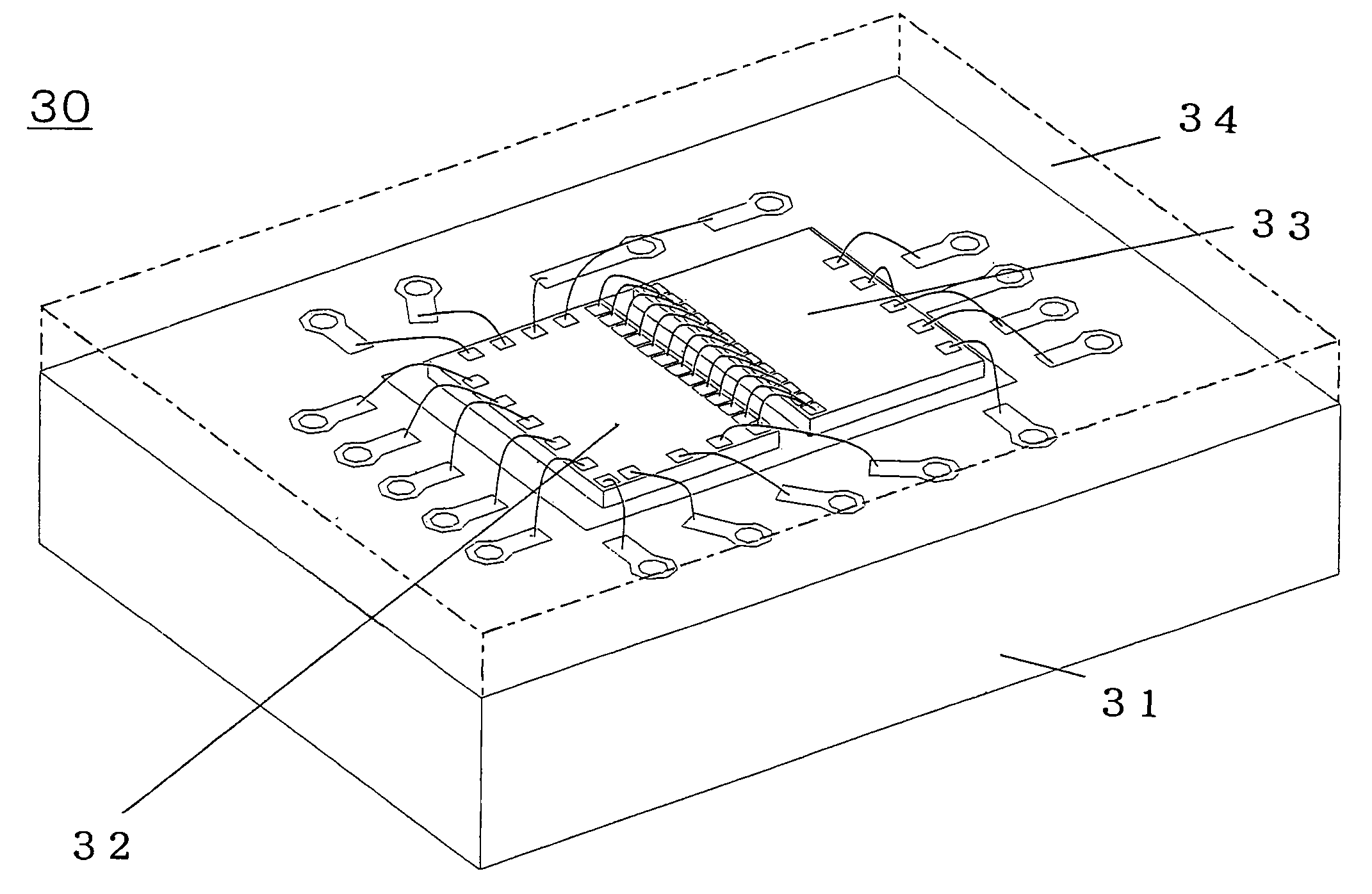
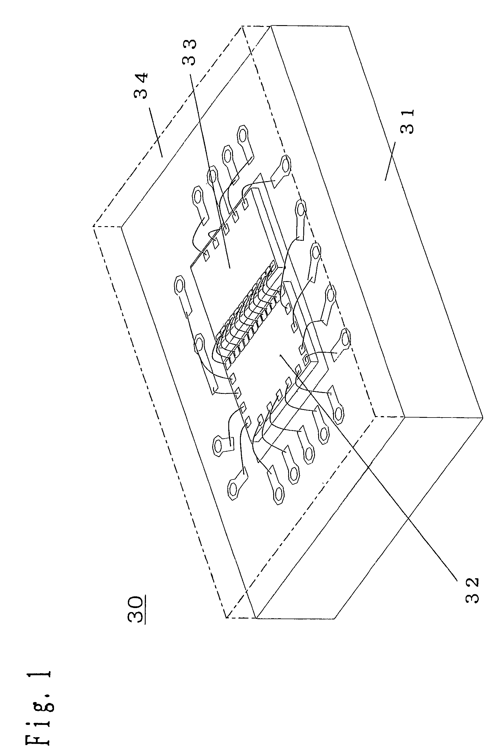
[0087]FIG. 1 is a perspective view of an antenna switch module 30 according to a first embodiment of the present invention. The antenna switch module 30 according to the first embodiment is comprised of a dielectric layered body 31 obtained by laminating and integrally burning a plurality of dielectric layers and a switch semiconductor chip 32 and a logic semiconductor chip 33 mounted on a top surface of the dielectric layered body 31. Electrode patterns are formed on the top surface, under surface and inside of the dielectric layered body 31 respectively. The portion indicted by a dashed line in the upper part of the dielectric layered body 31 in FIG. 1 is the portion to be resin-sealed, and FIG. 1 is a diagram seeing through this resin 34 portion.

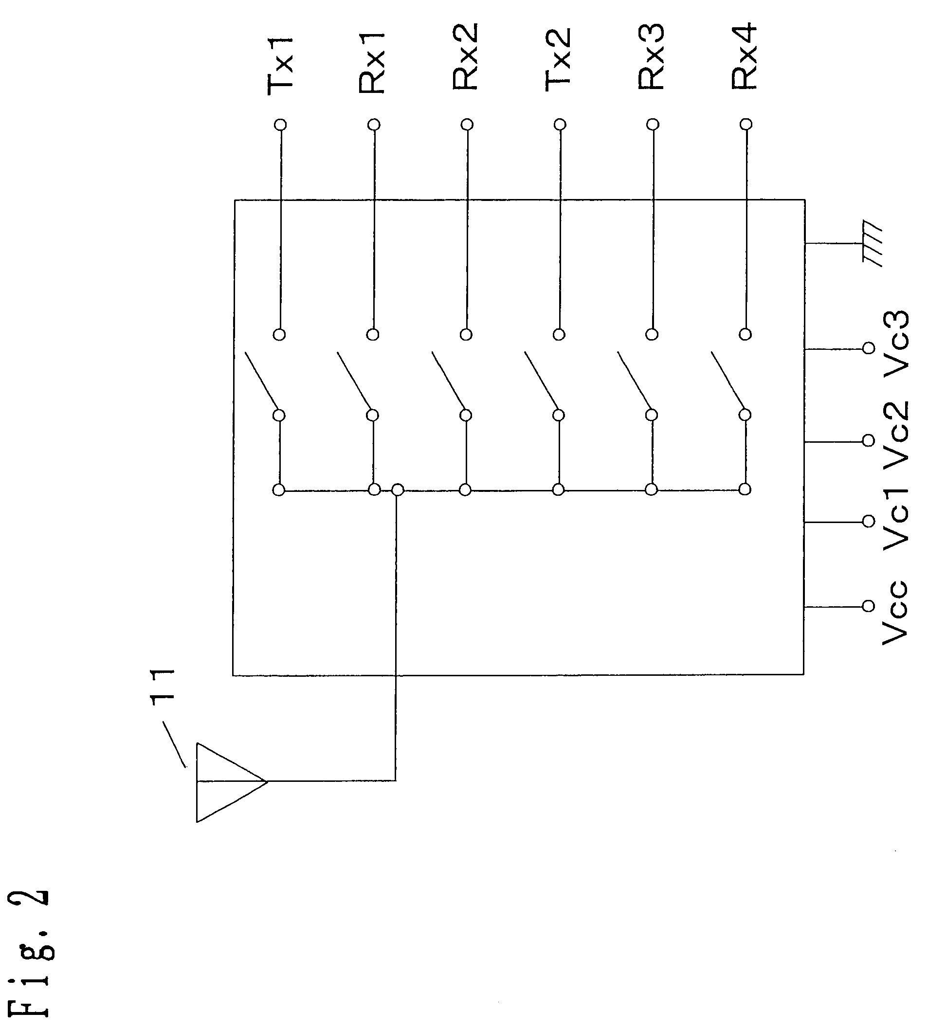
[0088]FIG. 2 is a block diagram of an SP6T (Single-Pole 6-Throw) antenna switch of the antenna switch module 30 according to the first embodiment. The SP6T antenna switch in FIG. 2 has a function of switching a route fro...

second embodiment

(Second Embodiment)

[0135]The antenna switch module according to a second embodiment will be described by referring to the drawings.

[0136]FIG. 9 is a perspective view of an antenna switch module 50 according to the second embodiment, and it partially shows a sectional view. The antenna switch module 50 according to the second embodiment is produced just like the antenna switch module 30 according to the first embodiment. A dielectric layered body 51 is comprised of a plurality of dielectric layers as the dielectric sheets of the present invention as with the dielectric layered body 31 of the first embodiment.

[0137]The dielectric layered body 51 has a high-frequency filter 37 formed by an internal electrode pattern 35 and a via hole electrode 36 formed by printing the high-frequency filter 37 being placed, below an earthed electrode pattern Gp5 and capacitor electrode patterns Cp11 to Cp16. The high-frequency filter 37 referred to here is a low-pass filter connected between the antenn...


PUM


Abstract

To realize high pressure-tightness and improvement in a high-frequency characteristic due to a low impedance between a shunt FET and a ground of a FET switch circuit. An antenna switch module comprising a switch circuit for switching between transmitting and receiving of a signal between an antenna and a transmitting portion and / or a receiving portion and having a shunt circuit, wherein a capacitor of the shunt circuit of the switch circuit is provided to a dielectric layered body, and remaining elements of the switch circuit are provided to semiconductor chips mounted on the dielectric layered body.

Description

BACKGROUND OF THE INVENTION[0001]1. Filed of the Invention[0002]The present invention relates to an antenna switch module, an all-in-one communication module, a communication apparatus and a method for manufacturing the antenna switch module. For instance, it relates to antenna switch modules for high-frequency and high-power signals.[0003]2. Related Art of the Invention[0004]In recent years, there has been a demand for a portable telephone supporting a multi band capable of using a plurality of methods. The reason for this is an expanding user base of mobile communication such as portable telephones and globalization. For instance, there is a demand for a triple-band portable telephone using three communication methods of different frequency bands of ESGM (Enhanced-Global System for Mobile Communication) method mainly used in Europe, a DCS (Digital Cellular System) method increasingly used in conjunction with the expanding user base of portable telephones and a PCS (Personal Commun...

Claims


Application Information

Patent Timeline
Patent Type & Authority Patents(United States)
IPC IPC(8): H04B1/44H01P1/15
CPCH01P1/15A01C3/04A01C3/066A01B63/108
Inventor ADACHI, MASAKAZUURIU, KAZUHIDEISHIZAKI, TOSHIO
Owner PANASONIC CORP
Why Eureka
Try Eureka