Method for pre-applied thermoplastic reinforcement of electronic components

a technology of electronic components and thermoplastics, applied in the direction of printed circuit non-printed electric components association, sustainable manufacturing/processing, final product manufacturing, etc., can solve the problems of uneconomical high-volume manufacturing, unsuitable for high-volume manufacturing, and large difficulty in uniform application of conventional underfill materials during manufacturing

Inactive Publication Date: 2005-12-27
HENKEL KGAA
View PDF23 Cites 10 Cited by
  • Summary
  • Abstract
  • Description
  • Claims
  • Application Information

AI Technical Summary

Problems solved by technology

Due to the differences in the coefficient of thermal expansion for the electronic component, the interconnect material, and the substrate, this thermal cycling can stress the components of the assembly and cause it to fail.
A drawback of capillary underfill is that its application requires several extra steps and is thus not economical for high volume manufacturing.
One limitation of the no flow underfill process is that the substrate and components must be pre-dried to avoid excessive voiding within the underfill that will lead to solder extrusion that ultimately may create a short-circuit to another connection.
This process is unwieldy for high volume manufacturers.
There is often great difficulty during manufacturing in uniformly applying conventional underfill materials.
The limitation to applying underfill to the bottom surface is that, in most cases, the underfill must contact at least a portion of the solder bump array.
This creates difficulties in creating a robust process that will not adversely affect the performance of the solder joints.

Method used


Image

  • Method for pre-applied thermoplastic reinforcement of electronic components
  • Method for pre-applied thermoplastic reinforcement of electronic components
  • Method for pre-applied thermoplastic reinforcement of electronic components

Examples


Embodiment Construction

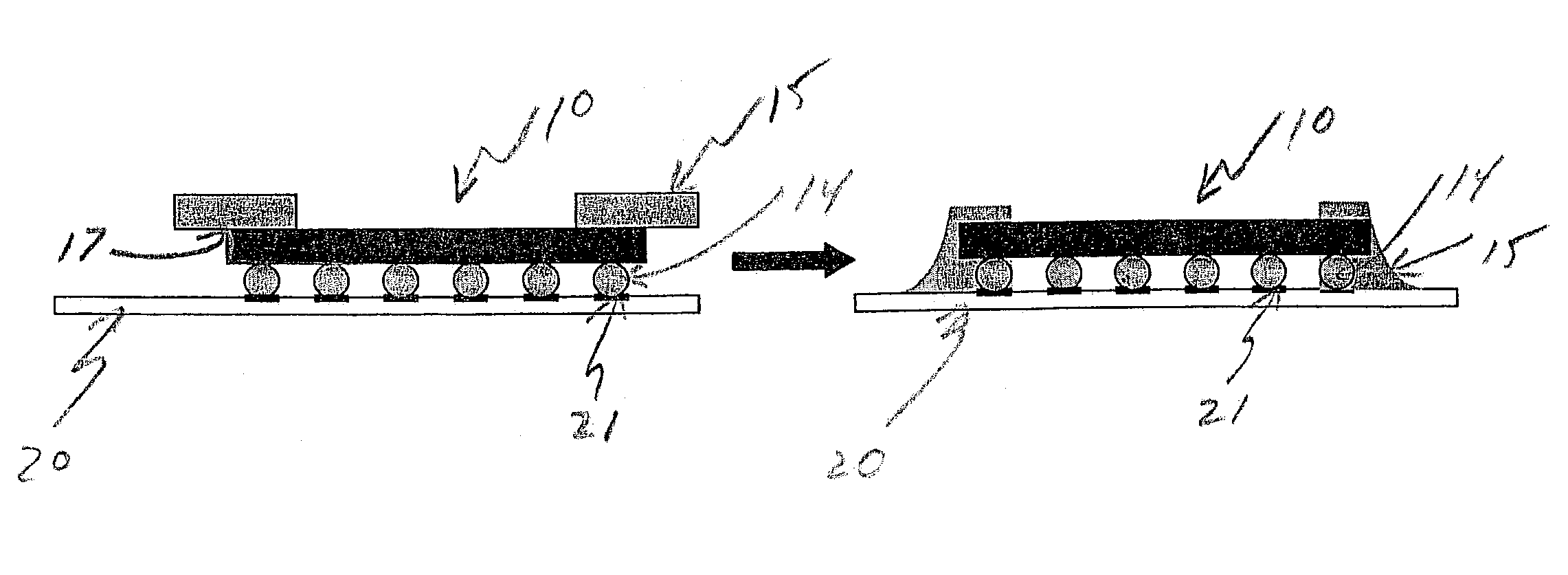
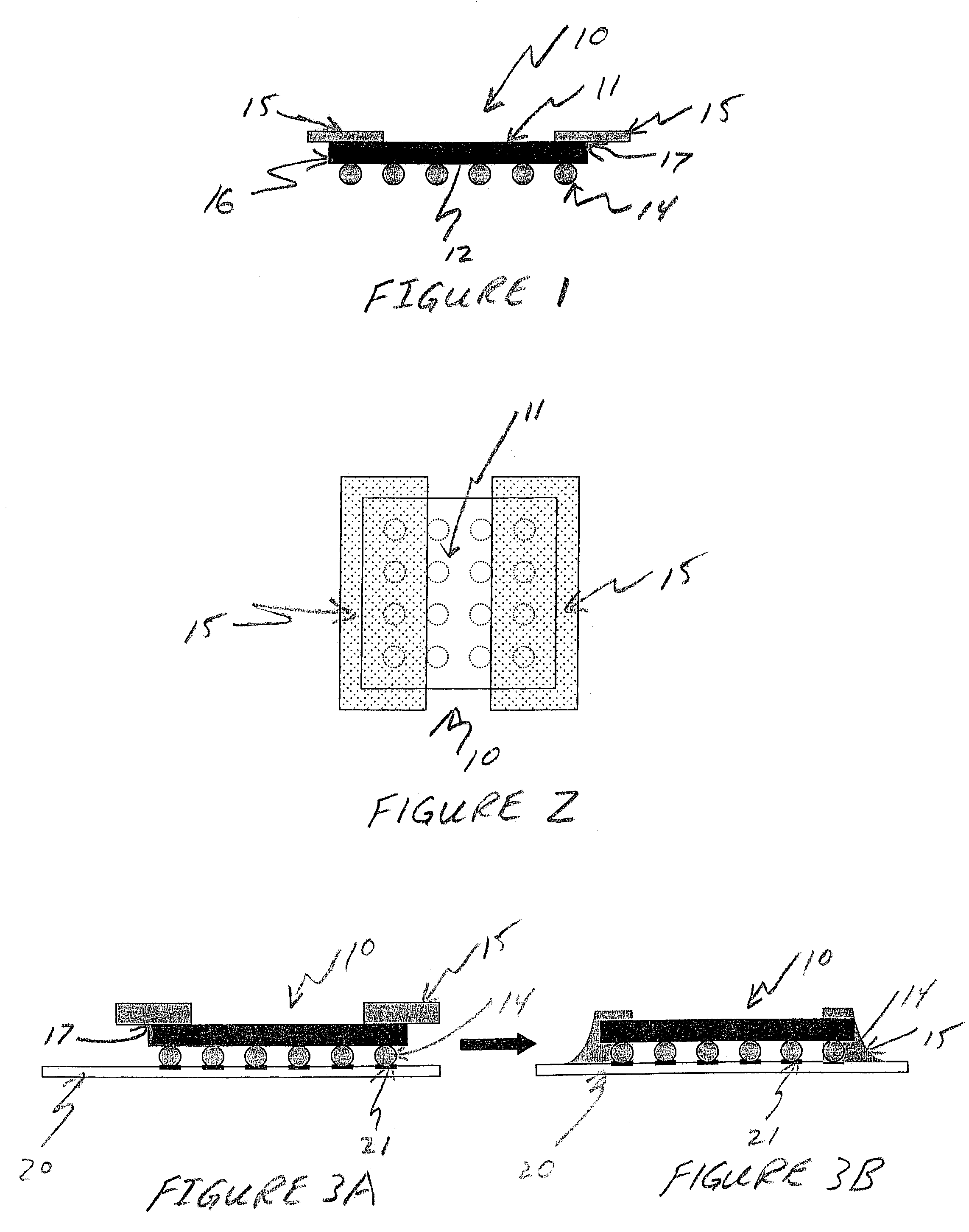
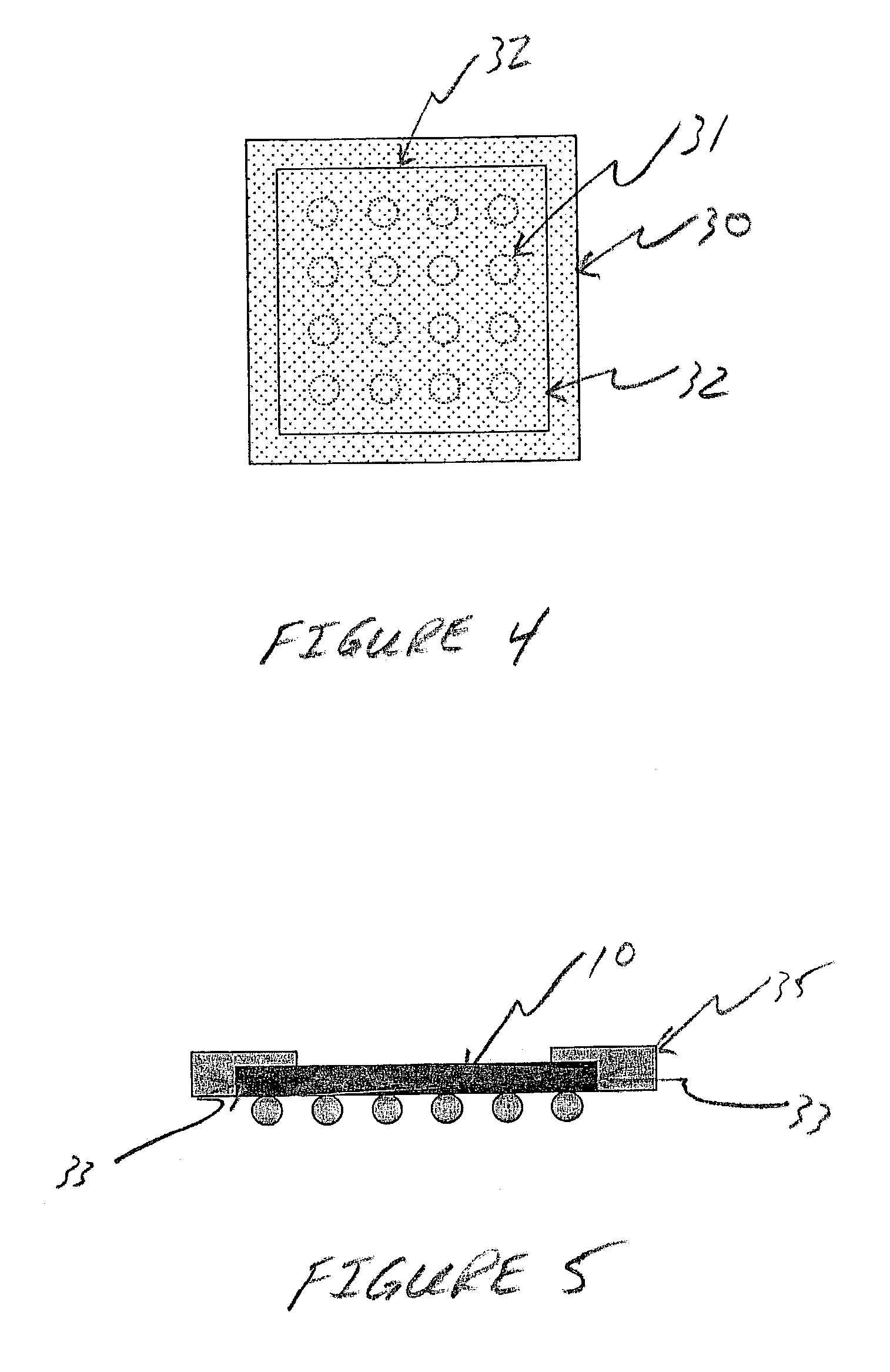
[0018]The pre-applied underfill of the present invention is preferably a film that is applied directly to the top and / or sides of a surface mount component, either before or after the component is attached to a substrate. The application of the underfill in this manner allows the component manufacturer to apply the underfill and thus eliminates the need for the circuit assembler to apply underfill. The circuit assembler could also apply the underfill of the invention as an alternative to conventional underfill. The underfill material is preferably a thermoplastic film reinforcement that is applied to the top and / or sides of an electronic component such as an area array device including CSP's, BGA's or flip chips, at any point before the reflow process and overhangs or extends beyond the sides of the component. While CSP's and BGA's are used throughout the description, it is to be understood that the pre-applied underfill of the present invention may be utilized with any form of surf...


PUM

PropertyMeasurementUnit
temperatureaaaaaaaaaa
melting pointaaaaaaaaaa

Abstract

A method for utilizing one or more pre-formed underfill compositions in the application of surface mount components, most commonly chip scale packages (CSP's), to substrates for use in electronic devices. The pre-formed underfill of the invention is applied directly to the top and / or sides of the CSP before the reflow process and softens during reflow to flow across the circuit / board gap. One underfill composition utilized for this method comprises a thermoplastic film system that provides a coating on the component that is smooth and non-tacky. The film may be applied selectively to parts of the CSP such that it overhangs the top of the component and upon reflow flows over the edge of the CSP to form a connection with the substrate. A second pre-applied underfill composition or solder paste may be applied as an adhesive to provide sufficient tack in order to hold the electronic assembly together during the assembly process and to serve as a flux to facilitate solder wetting.

Description

FIELD OF THE INVENTION[0001]The present invention is related to a method for the use of pre-applied thermoplastic underfill to electronic devices.BACKGROUND OF THE INVENTION[0002]This invention relates to a method of using pre-applied thermoplastic underfill in electronic devices. The underfill is used to protect and reinforce the interconnections between electronic components and substrates in microelectronic devices. Microelectronic devices contain multiple types of electrical circuit components, mainly transistors assembled together in integrated circuit (IC) chips, but also resistors, capacitors, and other components. These electronic components are interconnected to form the circuits, and eventually are connected to and supported on a carrier or a substrate, such as a printed wire board. The integrated circuit component may comprise a single bare chip, a single encapsulated chip, or an encapsulated package of multiple chips. The single bare chip can be attached to a lead frame,...

Claims


Application Information

Patent Timeline
Patent Type & Authority Patents(United States)
IPC IPC(8): H05K3/30
CPCH05K3/305H01L24/31H01L2924/19041Y10T29/49131H05K2201/0129H05K2201/10734H05K2201/10977H05K2201/10984H01L2224/16H01L2224/73203H01L2224/83951H01L2924/01005H01L2924/01013H01L2924/01027H01L2924/01032H01L2924/01047H01L2924/01049H01L2924/0105H01L2924/01051H01L2924/01079H01L2924/01082H01L2924/01322H01L2924/14H01L2924/01006H01L2924/01033H01L2924/0132H01L2924/19043Y10T29/49117Y10T29/4913Y10T29/49144H01L2224/29111H01L2224/2919H01L2924/00015H01L2924/00014H01L2924/12042Y02P70/50H01L2924/00H01L2224/0401
Inventor MORGANELLI, PAULPEARD, DAVIDSHAH, JAYESHKATZE, DOUGLAS
Owner HENKEL KGAA
Why Eureka
Try Eureka