Process for controlling performance characteristics of a negative differential resistance (NDR) device

a technology of negative differential resistance and performance characteristics, which is applied in the testing/measurement of individual semiconductor devices, semiconductor/solid-state devices, instruments, etc., can solve the problems of inability to easily adjust the peak-to-valley ratio (pvr), and the limitations of the prior art to date, so as to achieve the effect of maximum “source side” trapping and faster switching speed

Inactive Publication Date: 2005-12-27
SYNOPSYS INC
View PDF114 Cites 3 Cited by
  • Summary
  • Abstract
  • Description
  • Claims
  • Application Information

AI Technical Summary

Benefits of technology

[0116]An advantage of the present invention is that the onset of NDR behavior can be controlled through selecting a target trap energy level. In turn, the trap energy level can be engineered through suitable process control parameters such as through selection of a particular impurity species and / or trapping layer dielectric.
[0117]A mask can be used to selectively form the charge trapping region in those areas 1015 where an NDR element is to be formed, and in some instances so that it does not extend across an entire region 1015 of substrate 1000, but is instead limited to some smaller area corresponding to a later gate region of an NDR FET, or even a limited portion of such gate region. In some cases, for example, it may be desirable to form a trapping region only near a source region, or only near a drain region, depending on the expected device biasing and operational characteristics. To maximize “source side” trapping, for example, charge traps can be selectively arranged to extend from a source region, and not extend entirely through the channel to a drain side. A variable distribution of traps might be employed along a length of the channel so as to effectuate a trapping rate that varies correspondingly and results in a faster switching speed.
[0118]It is expected that routine experimentation will yield a variety of trap distributions for optimizing different characteristics of an NDR FET, such as switching speed, VNDR, noise immunity, leakage, subthreshold swing, Vt, etc. Thus it will be understood by those skilled in the art that while it is shown as extending throughout all of region 1015, the invention is not limited to such implementations, and in fact a variety of charge trapping structures may be used advantageously for different applications.
[0119]Thus, the present detailed description continues with a discussion of FIG. 8, which is a schematic cross-sectional view showing the step of forming an initial insulating layer (after sacrificial oxide layer 1018 is removed) on the surface of the substrate in a first region 1015 where an NDR FET of a preferred embodiment is to be formed as part of step 425 described above. This initial insulating layer 1020 functions as part of a gate insulator for a to-be-formed NDR FET, and can also serve as a charge trapping region for such NDR FET. It is formed on the surface of substrate 1000 in active areas 1015 by one of several well-known techniques, including thermal oxidation of silicon. Physical vapor deposition and chemical vapor deposition can also be used. This electrically insulating layer 1020 can consist entirely or in part of SiO2, SiOxNy, Si3N4, or a high-permittivity dielectric material such as metal oxide or metal silicate or their laminates, or, of course, as a combination of one or more different material layers.
[0120]As with other processing steps noted herein, an advantage of the present invention lies in the fact that this layer (as patterned later) can be shared by both conventional and NDR FET devices. Alternatively viewed, from a process integration impact, the existence of such layer in non-NDR regions during these NDR FET formational steps does not negatively impact the structure, performance or reliability of any non-NDR elements. Nonetheless, in some applications it may be desirable to mask and etch layer 1020 in those areas where non-NDR elements are to be formed, so that charge trapping regions are not formed later across all regions of the substrate.
[0121]In an alternate embodiment, traps are formed by directly implanting the gate insulator layer 1020 using a combination of energies and species that ensure a high concentration at a channel interface and a low concentration in a bulk region of layer 1020.

Problems solved by technology

Furthermore, the prior art to date has been limited generally to devices in which the peak-to-valley ratio (PVR) is not easily adjustable.
Alternatively, the ability to control PVR during normal operation of a device would also be useful, but is generally not possible with current NDR technologies.

Method used


Image

  • Process for controlling performance characteristics of a negative differential resistance (NDR) device
  • Process for controlling performance characteristics of a negative differential resistance (NDR) device
  • Process for controlling performance characteristics of a negative differential resistance (NDR) device

Examples


Embodiment Construction

[0068]A preferred embodiment of the invention is now described with reference to the Figures provided herein. It will be appreciated by those skilled in the art that the present examples are but one of many possible implementations of the present teachings, and therefore the present invention is not limited by such.

[0069]The present invention is expected to find substantial uses in the field of integrated circuit electronics as an additional fundamental “building block” for digital memory, digital logic, and analog circuits. Thus, it can be included within a memory cell, within a Boolean function unit, and similar such environments.

Brief Summary of Prior Art

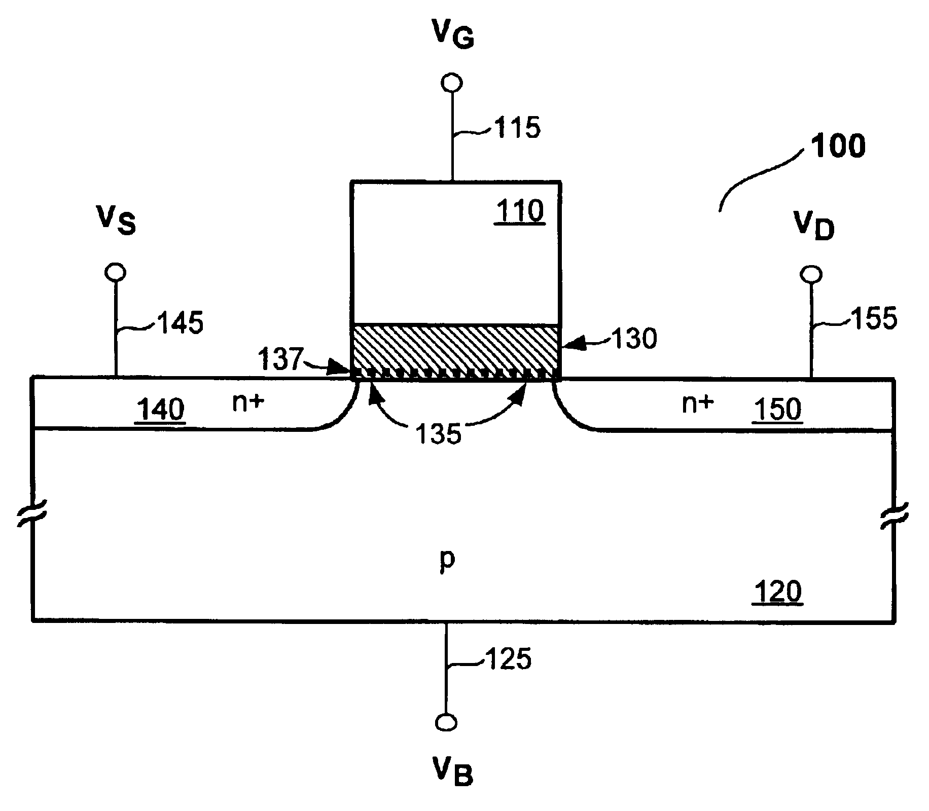
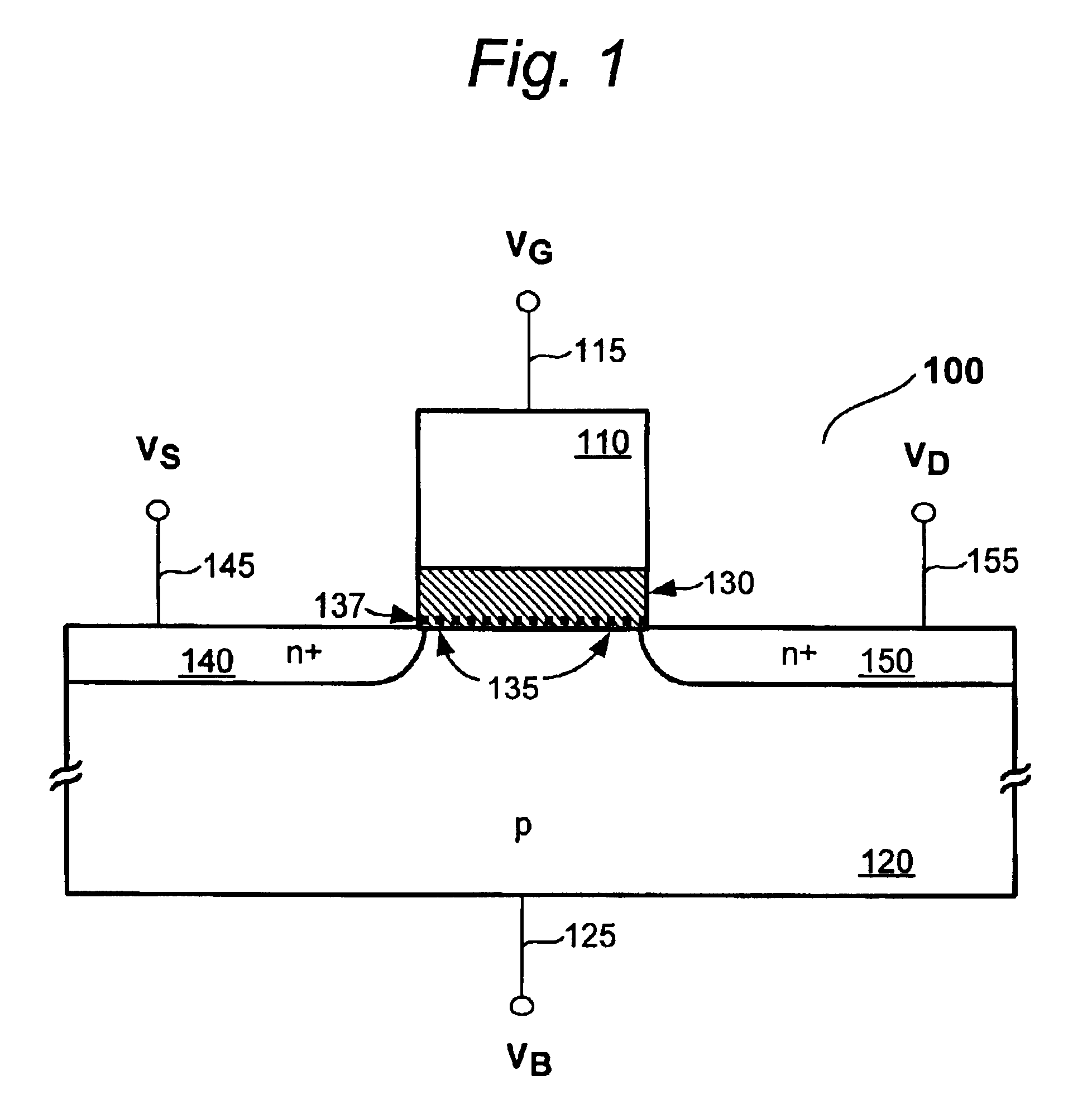
[0070]FIG. 1 shows a prior art NDR FET 100 of the type described in the King et al. applications noted earlier. This device is essentially a silicon based MISFET that includes an NDR characteristic as well. Thus, the features of device 100 are created with conventional MOS based FET processing, modified where appropriate as to in...


PUM


Abstract

A variety of processes are disclosed for controlling NDR characteristics for an NDR element, such as peak-to-valley ratio (PVR), NDR onset voltage (VNDR) and related parameters. The processes are based on conventional semiconductor manufacturing operations so that an NDR device can be fabricated using silicon based substrates and along with other types of devices.

Description

CROSS REFERENCE TO RELATED APPLICATIONS[0001]The present application is related to the following applications, all of which are filed simultaneously herewith, and which are hereby incorporated by reference as if fully set forth herein:[0002]Method of Forming A Negative Differential Resistance Device; Ser. No. 10 / 324,735;[0003]Integrated Circuit Having Negative Differential Resistance (NDR) Devices With Varied Peak-to-Valley Ratios (PVRs); Ser. No. 10 / 321,031.FIELD OF THE INVENTION[0004]This invention is directed to processes for controlling performance characteristics of negative differential resistance elements, particularly peak-to-valley (PVR) ratios and NDR onset voltages for NDR field-effect transistor devices.BACKGROUND OF THE INVENTION[0005]Silicon based devices that exhibit a negative differential resistance (NDR) characteristic have long been sought after in the history of semiconductor devices. A new type of CMOS compatible, NDR capable FET is disclosed in the following Ki...

Claims


Application Information

Patent Timeline
Patent Type & Authority Patents(United States)
IPC IPC(8): H01L21/265H01L21/28H01L21/336H01L21/8238H01L21/8244H01L21/8246H01L21/84H01L27/105H01L27/11H01L27/115H01L27/12H01L29/423H01L29/51
CPCH01L27/11H01L27/11568H01L29/42332H01L29/42348H01L29/513H01L29/66833H01L29/7881H01L29/792H01L21/28176H01L21/28185H01L21/28194H01L21/28282H01L21/823857H01L27/0629H01L27/105H01L27/115H01L27/1203H01L29/517H01L29/518H01L21/2652H01L21/823462H01L21/84H01L29/40117H10B10/00H10B43/30H10B69/00H01L21/26513
Inventor KING, TSU-JAE
Owner SYNOPSYS INC
Why Eureka
Try Eureka