Patterned wafer inspection method and apparatus therefor

a technology of patterned wafers and inspection methods, applied in semiconductor/solid-state device testing/measurement, material analysis using wave/particle radiation, instruments, etc., can solve the problems of limiting the inspection time, and limiting the high speed. , to achieve the effect of shortening the inspection time of the pattern comparison inspection method

Inactive Publication Date: 2005-12-27
HITACHI LTD
View PDF11 Cites 27 Cited by
  • Summary
  • Abstract
  • Description
  • Claims
  • Application Information

AI Technical Summary

Benefits of technology

[0008]Therefore, an object of the present invention is to shorten the test required time of the pattern comparison inspecting method using an electron beam such as equal to or less than that of the conventional optical inspecting method.
[0012]Namely, in the patterned wafer inspection method of the present invention, an electron beam from the electron source is sequentially irradiated to a plurality of irradiation regions (area regions) of the surface of a semiconductor sample as a so-called area beam, and enlarged images in the plurality of irradiation regions are sequentially formed by electron-optically imaging backscattering electrons from the plurality of irradiation regions or secondary electrons, and the enlarged images in the plurality of irradiation regions are sequentially converted to electrical image signals and stored, and a pattern defect in each of the aforementioned irradiation regions is detected by comparing the stored image signals in the plurality of irradiation regions with each other. According to this method, the conventional two-dimensional scanning by a spot beam in each irradiation region (area region) is not necessary, so that the inspection time can be greatly shortened and the defect test can be speeded up.
[0017]On the other hand, a method for setting so that the size of enlarged images on the surface of a semiconductor sample which can be obtained at the same time by irradiating an electron beam at the same time becomes almost equal to the size of the light receiving surface of the image detection device is simpler. On the other hand, by setting the size of the electron beam irradiation region so that the size of enlarged images on the surface of a semiconductor sample is made smaller than the size of the light receiving surface of the image detection device, scanning the electron beam on the surface of the semiconductor sample, then projecting the enlarged images overall the light receiving surface of the image detection device for a given period of time, and superimposing a signal for correcting the variation factors of irradiation position and irradiation range on the scanning signal of the electron beam, a method realizing higher precision may be available.
[0018]To decelerate an electron beam to be irradiated onto a semiconductor sample, make the energy value of the electron beam when it is irradiated onto the sample sufficiently smaller than the energy value before deceleration, and keep the energy dispersion of backscattering electrons generated from the sample surface by irradiation of the decelerated electron beam within a range that it will not affect the resolution of the imaging system, a negative potential is applied to the semiconductor sample. Or, by providing a filter for discriminating backscattering electrons generated by irradiation of the electron beam or secondary electrons in energy and imaging only backscattering electrons or secondary electrons with a specific energy width, the problem of high speed test can be solved and the resolution can be improved at the same time.

Problems solved by technology

When pattern defects in the manufacturing process of a semiconductor device are tested by such an optical inspecting method, residuals of a silicon oxide film through which light transmits and a photosensitive resist material cannot be detected.
However, since the electron beam is limited to a spot shape and this spot beam is two-dimensionally scanned on the surface of a sample, there is a limit to the high speed (shortening of the inspecting time).
There is also a limit to the large current of an electron beam to be used due to the brightness of the electron source used and space charge effect.
On the other hand, in the aforementioned conventional optical inspection apparatus, the test required time for an inspection area of 1 cm2 is very short such as about 5 seconds.

Method used


Image

  • Patterned wafer inspection method and apparatus therefor
  • Patterned wafer inspection method and apparatus therefor
  • Patterned wafer inspection method and apparatus therefor

Examples


embodiment 1

[0029

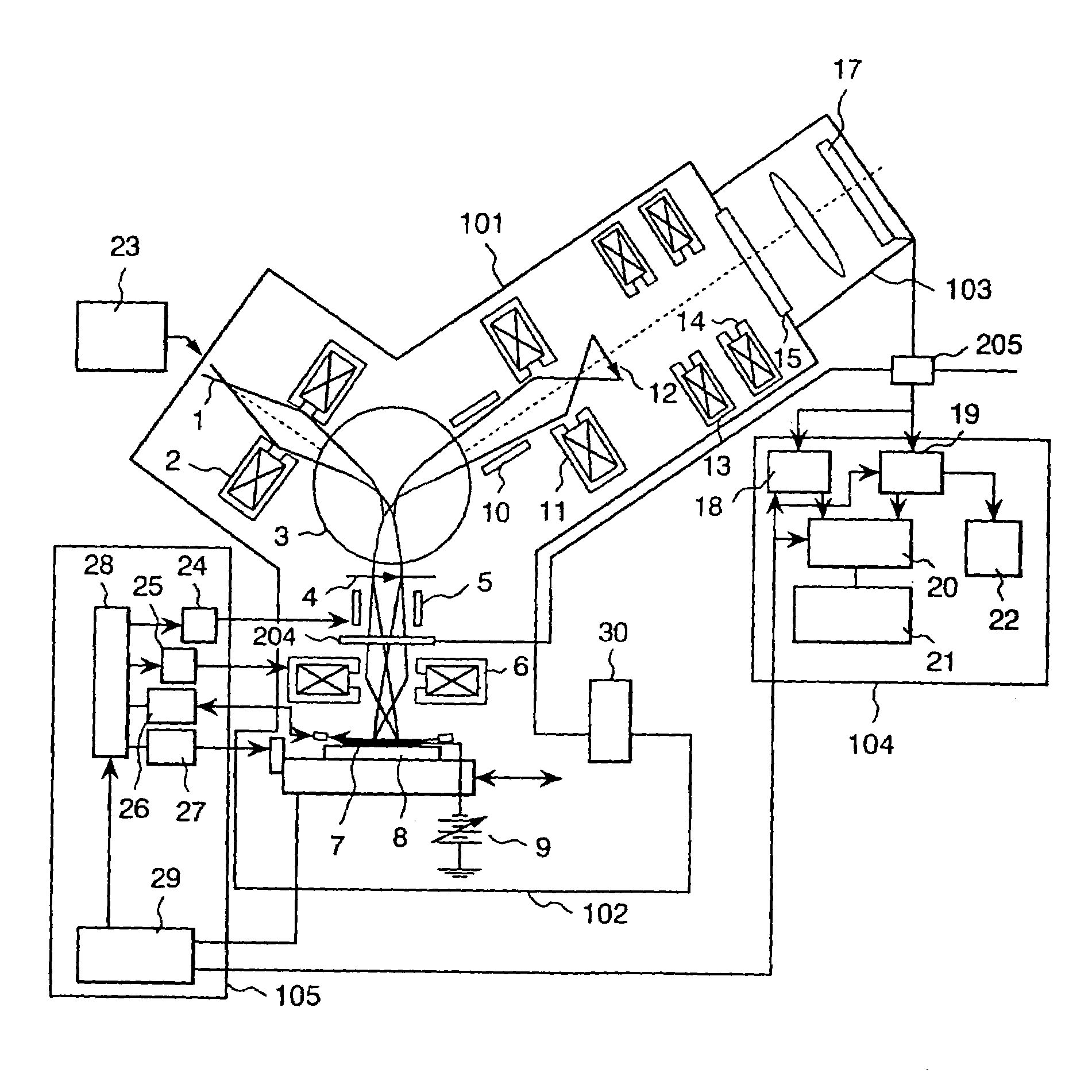
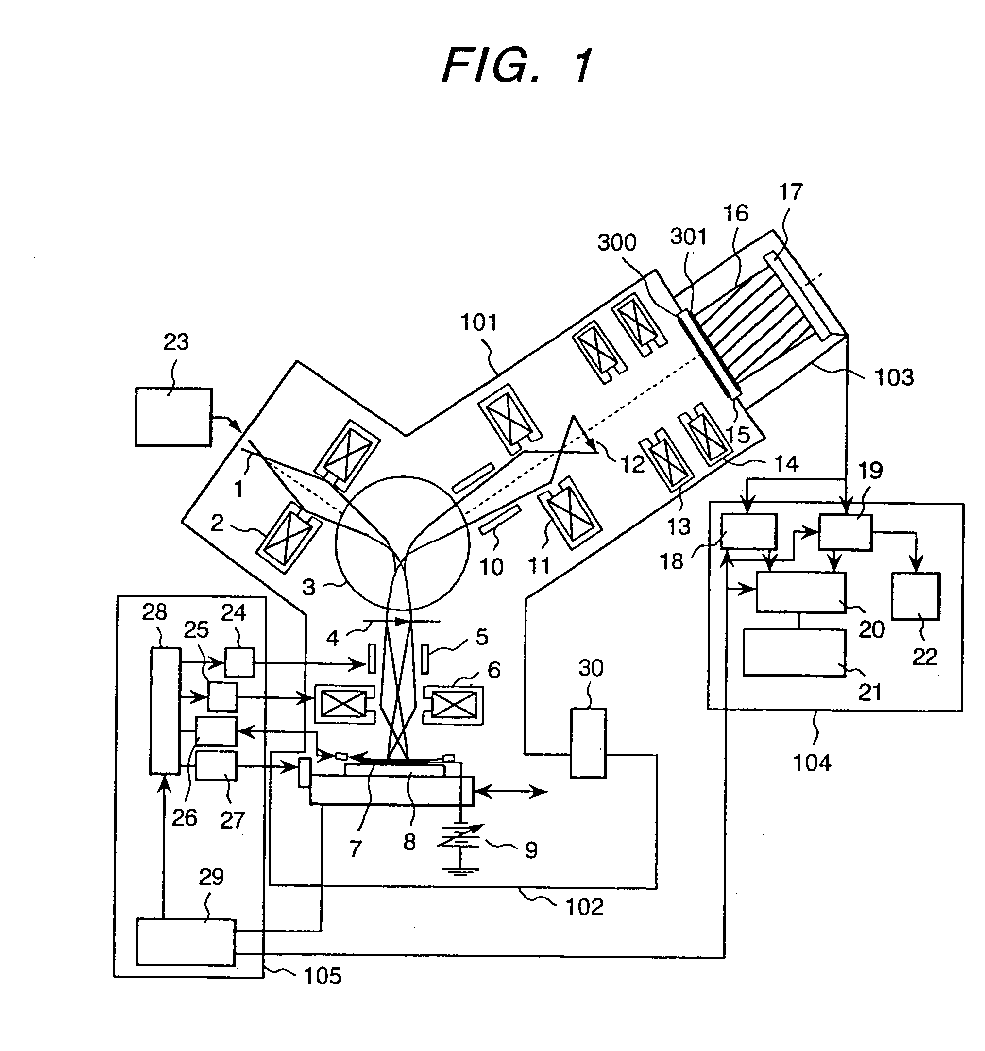
[0030]FIG. 1 shows a schematic view of the inspection apparatus which is an embodiment of the present invention. The inspection apparatus of the present invention broadly comprises an electron optical system 101, a sample chamber 102, an image detector 103, an image processor 104, and a controller 105.

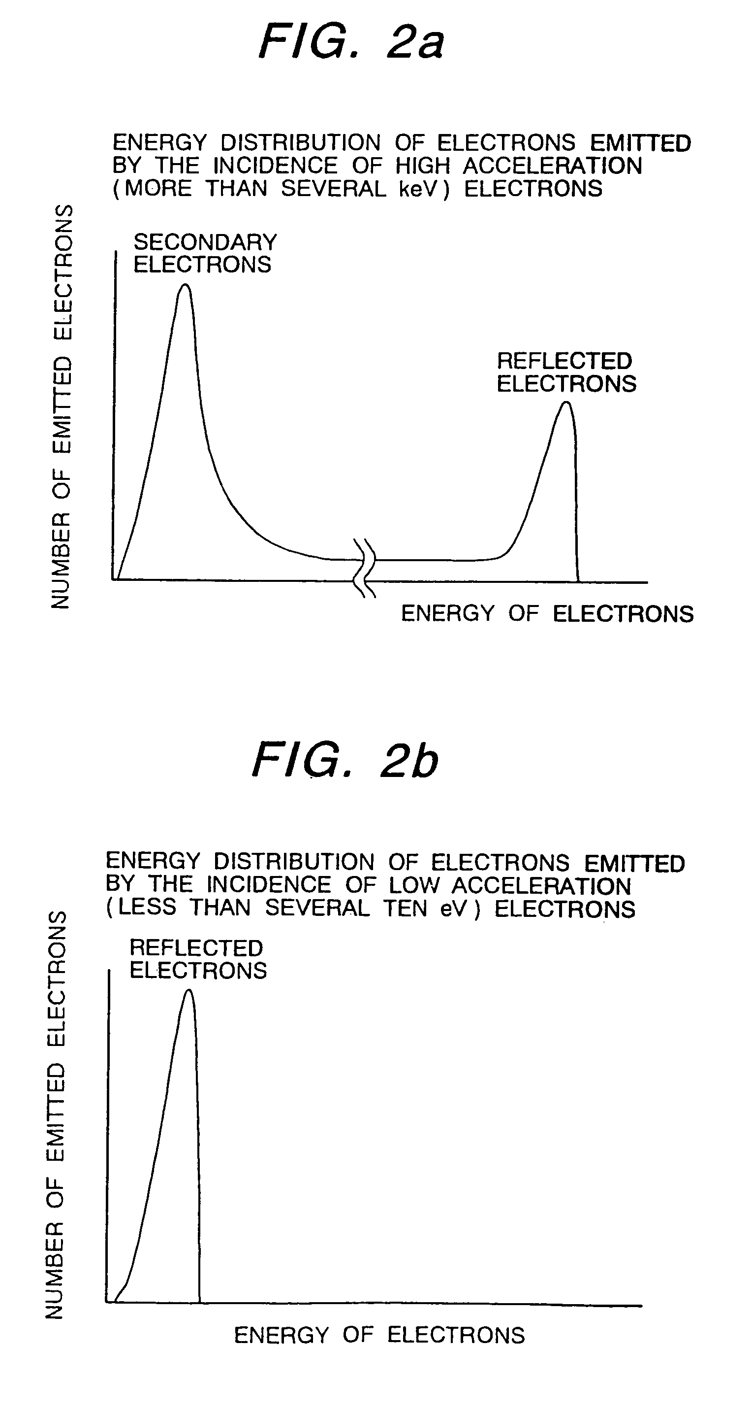
[0031]Firstly, the electron optical system 101 will be explained. An acceleration electron beam emitted from an electron source 1 which is given a negative high potential from an acceleration power source 23 is focused by a condenser lens 2 and irradiated onto an aperture 4 having a rectangular opening. The electron beam is deflected by an electromagnetic deflector 3 before it is irradiated onto the aperture 4. The electromagnetic deflector 3 is used to separate the path of an incoming electron beam from the electron source 1 from the path of a reflected electron (backscattering electron or secondary electron) beam from a sample. An incoming electron beam passing through the recta...

embodiment 2

[0056

[0057]In the aforementioned Embodiment 1, the area of the electron beam irradiation region of 1 shot is considerably large such as 100 μm×100 μm, so that a problem may arise that a distortion is generated in the periphery of the enlarged image of the semiconductor sample or that the beam current density in the irradiation region becomes ununiform. When an image distortion or ununiformity of current density is fixedly generated, it can be corrected by changing the fiber strand layout of the optical fiber bundle 16. The obtaining sensitivity of an image signal and weighting of the image process can be corrected. However, if they vary in time, it is hard to handle by those methods. In this embodiment, the irradiation region of 1 shot is a square of 5 μm and it is designed to prevent the problems of distortion and ununiformity of current density. The irradiation electron beam current is 5 μA per 1 shot. In this case, assuming the electron scattering efficiency η as 0.2, from the fo...

embodiment 3

[0063

[0064]In this embodiment, as a device for converting a sample surface image to an electric signal, a time accumulative CCD sensor is used. This sensor is called a TDI sensor and generally used in an optical inspecting apparatus. The constitution other than it is the same as that of the aforementioned Embodiment 2. The operation concept of the TDI sensor will be explained by referring to FIG. 5. The TDI sensor operates so as to move the charge generated according to the intensity of the light received by each light receiving region to the line in the x direction and sequentially add the charge generated according to the intensity of the light received by the moving destination at-the same time. Upon arrival at the last line of the light receiving surface, the TDI sensor outputs it to the outside as an electric signal.

[0065]Therefore, when the moving speed of the charge in the x direction is made equal to the moving speed of an image on the light receiving surface in the x direct...


PUM

PropertyMeasurementUnit
areaaaaaaaaaaa
sizeaaaaaaaaaa
diameteraaaaaaaaaa

Abstract

An electron beam (area beam) having a fixed area is irradiated onto the surface of a semiconductor sample, and reflected electrons from the sample surface are imaged by the imaging lens, and images of a plurality of regions of the surface of the semiconductor sample are obtained and stored in the image storage unit, and the stored images of the plurality of regions are compared with each other, and the existence of a defect in the regions and the defect position are measured. By doing this, in an apparatus for testing a pattern defect of the same design, foreign substances, and residuals on a wafer in the manufacturing process of a semiconductor apparatus by an electron beam, speeding-up of the test can be realized.

Description

[0001]This is a continuation application of U.S. Ser. No. 10 / 400,588, filed on Mar. 28, 2003 now U.S. Pat. No. 6,797,954 which is a continuation of application Ser. No. 09 / 164,366, filed Oct. 1, 1998, now abandoned.BACKGROUND OF THE INVENTION[0002]1. Field of the Invention[0003]The present invention relates to a method for testing the surface status of a sample (a semiconductor device, etc.) and apparatus therefor and particularly to an inspection method and apparatus therefor for imaging and inspecting fine pattern defects on the surface of a semiconductor device in high sensitivity and high resolution at high speed using an electron beam.[0004]2. Description of the Prior Art[0005]As an inspecting method for detecting defects of a circuit pattern formed on a wafer by comparison test in the manufacturing process of a semiconductor device, there is a method for obtaining images of two or more same kind of LSI patterns on one wafer using light, comparing these plurality of images, and...

Claims


Application Information

Patent Timeline
Patent Type & Authority Patents(United States)
IPC IPC(8): G01N23/225G01N23/20G01Q20/02G01Q30/02G01Q30/04G01Q30/20H01J37/26H01L21/027H01L21/66
CPCG01N23/225H01J37/244H01J37/26H01J37/29H01J2237/20228H01J2237/221H01J2237/2447H01J2237/24475H01J2237/24485H01J2237/24592H01J2237/2482H02B1/20H02B1/56H02P31/00
Inventor SHINADA, HIROYUKIYAJIMA, YUSUKEMURAKOSHI, HISAYAHASEGAWA, MASAKINOZOE, MARITAKAFUJI, ATSUKOSUGIYAMA, KATSUYAKURODA, KATSUHIROUMEMURA, KAORUUSAMI, YASUTSUGU
Owner HITACHI LTD
Why Eureka
Try Eureka