

Package substrate for improving electrical performance
a technology of electrical performance and packaging substrate, which is applied in the direction of electrical apparatus, semiconductor devices, and semiconductor/solid-state device details, etc., can solve the problems of impedance of electrical performance of the package substrate, and the inability to electrically connect the holes to the ground/power plane, etc., and achieve the effect of easy formation
- Summary
- Abstract
- Description
- Claims
- Application Information
AI Technical Summary
Benefits of technology
Problems solved by technology
Method used
Image

Examples
Embodiment Construction
[0010]Referring to the attached drawings, the present invention will be described by means of the embodiments below.
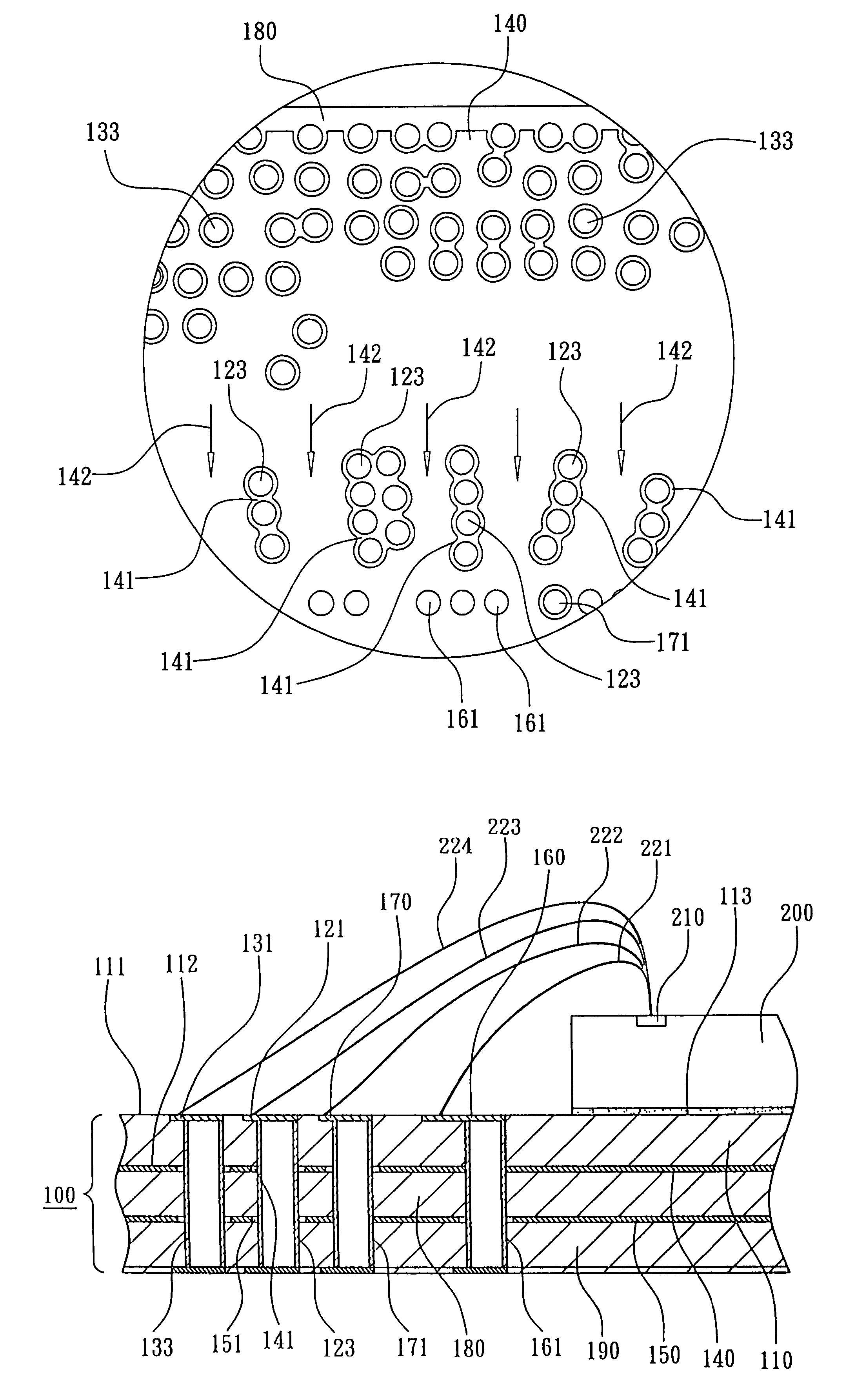
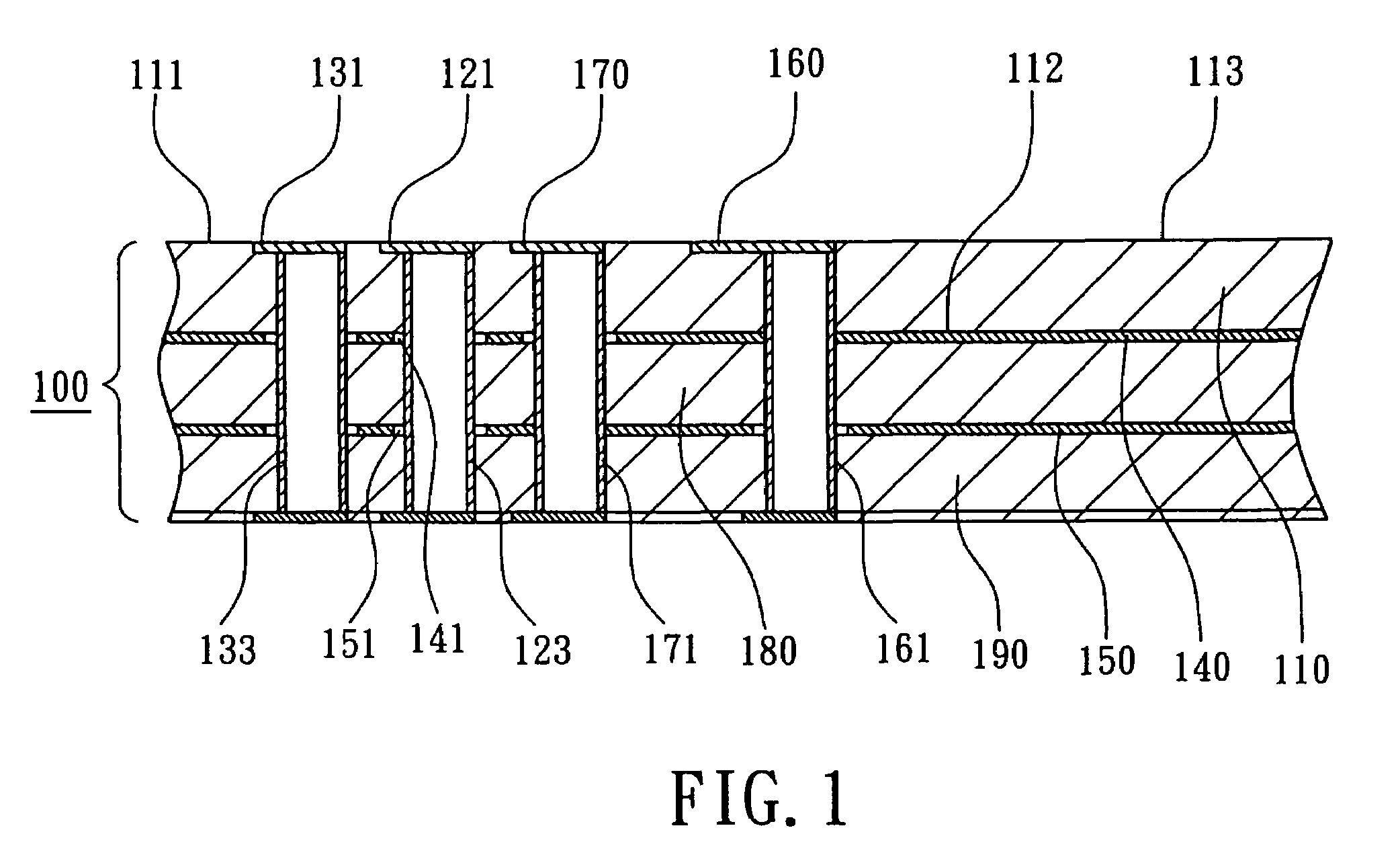
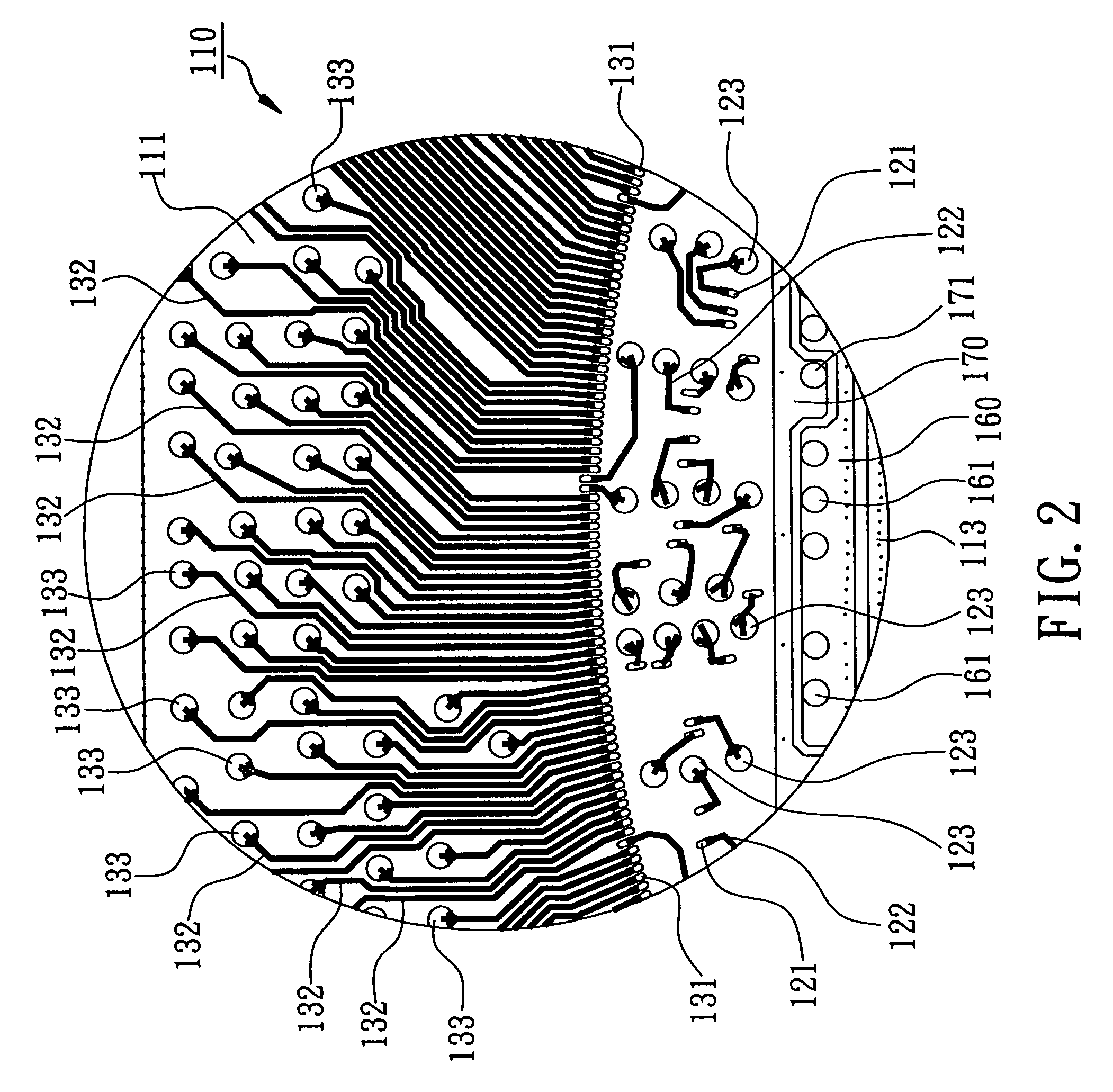
[0011]As shown in FIG. 1, according to the present invention a package substrate 100 for improving electrical performance mainly comprises a first insulating layer 110, a wiring layer and at least a ground / power layer (which includes a ground layer 140 and a power layer 150). The first insulating layer 110 is made of glass fiber reinforced resin of FR-4, FR-5, BT resin, or a soft insulating layer, such as polyimide. The first insulating layer 110 has a top surface 111 and a bottom surface 112. The top surface 111 includes a chip-attaching region 113 for attaching a semiconductor chip 200 (referring to FIGS. 1 and 4). The wiring layer is formed on top surface 111 of the first insulating layer 110. As shown in FIG. 1 and FIG. 2, the wiring layer includes a plurality of inner fingers 121, a plurality of outer fingers 131 and a plurality of traces 122, 132. The inner finge...
PUM
 Abstract
Description
Claims
Application Information