Method and system for determining optimum optical proximity corrections within a photolithography system

a photolithography system and optical proximity technology, applied in the field of integrated circuit fabrication, can solve the problems of tedious manual determination by trial and error and prone to human error, and achieve the effect of efficient and accurate determination

Inactive Publication Date: 2006-01-03
ADVANCED MICRO DEVICES INC
View PDF2 Cites 9 Cited by
  • Summary
  • Abstract
  • Description
  • Claims
  • Application Information

AI Technical Summary

Benefits of technology

[0016]In this manner, optimum optical proximity corrections (OPC) are efficiently and accurately determined for a pattern of polygons by the use of the array of mask areas on the reticle and the computer system with the database.

Problems solved by technology

However, such a manual determination by trial and error is tedious and prone to human error as such a process is repeated for different integrated circuit processes and different photolithography systems.

Method used


Image

  • Method and system for determining optimum optical proximity corrections within a photolithography system
  • Method and system for determining optimum optical proximity corrections within a photolithography system
  • Method and system for determining optimum optical proximity corrections within a photolithography system

Examples


Embodiment Construction

[0029]According to a general aspect of the present invention, optimum optical proximity corrections (OPC) are determined for an IC (integrated circuit) process and for a photolithography system. The optimum optical proximity corrections (OPC) typically would vary depending on the IC (integrated circuit) process since dimensions and density desired for an IC (integrated circuit) process varies. In addition, the optimum optical proximity corrections (OPC) typically would vary depending on the photolithography system since different components within different photolithography systems would cause different non-linear distortions on the patterned polygons on the semiconductor wafer.

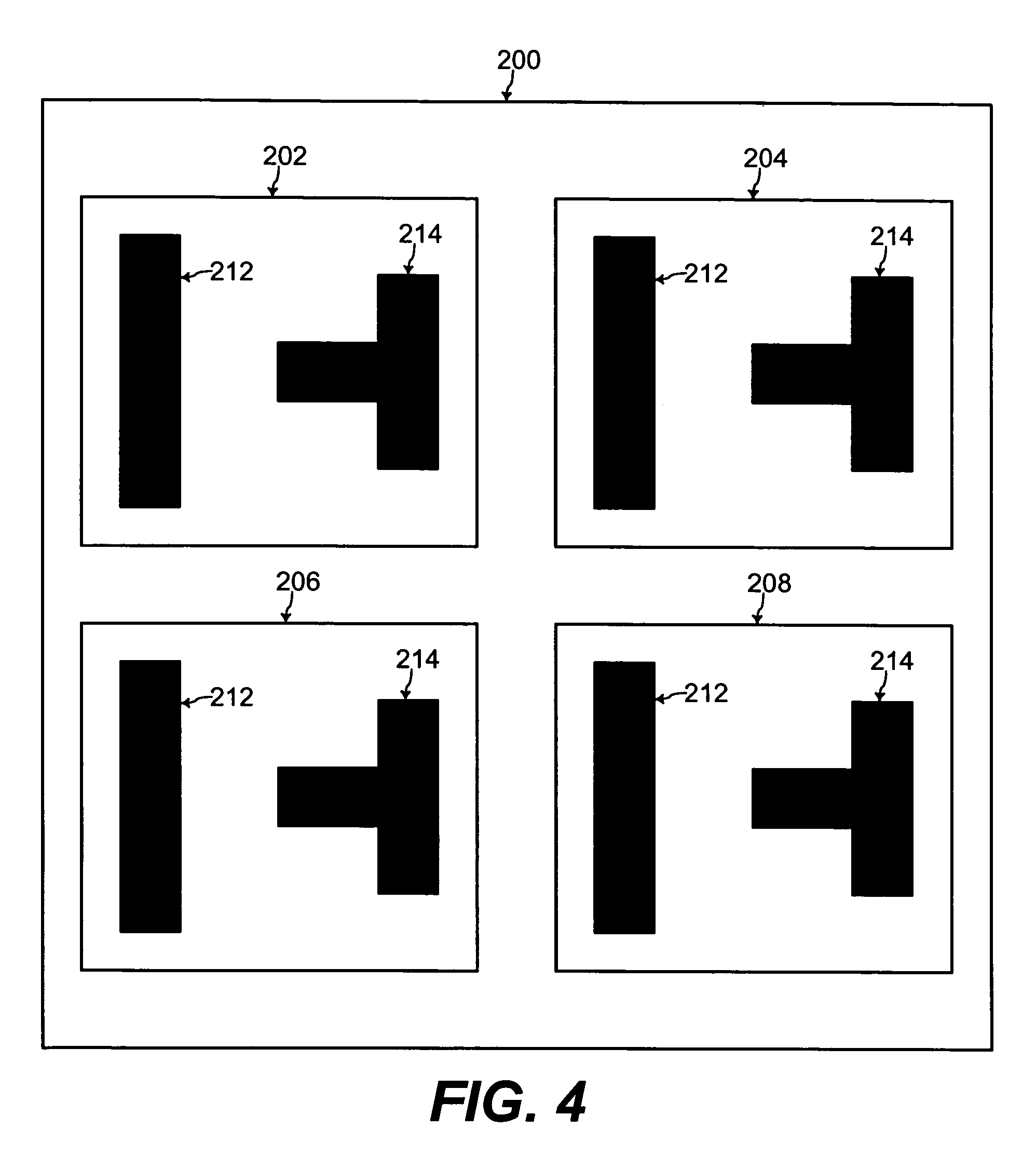
[0030]FIG. 7 shows a flow-chart of steps of operation for determining optimum optical proximity corrections (OPC) according to an embodiment of the present invention. Referring to FIG. 4, for determining optimum optical proximity corrections (OPC), an array of mask areas are formed on a reticle 200 including ...


PUM

PropertyMeasurementUnit
wavelengthaaaaaaaaaa
areaaaaaaaaaaa
microscopyaaaaaaaaaa

Abstract

For determining optimum optical proximity corrections (OPCs) for a mask pattern, mask areas are formed on a reticle with each mask area having the mask pattern of polygons that are modified with respective OPCs perturbations. A respective patterned area is fabricated on a semiconductor wafer from each mask area of the reticle. A respective microscopy image of each respective patterned area is generated to determine a respective error function for each mask area by comparing a desired image of the mask pattern and the respective microscopy image. The optimum OPCs are determined as the respective OPCs perturbations corresponding to one of the mask areas having the respective error function that is a minimum of the mask areas.

Description

[0001]This is a divisional of an earlier filed copending patent application, with Ser. No. 10 / 161,450 filed on May 31, 2002, now U.S. Pat. No. 6,824,937, for which priority is claimed. This earlier filed copending patent application with Ser. No. 10 / 161,450 is in its entirety incorporated herewith by reference.TECHNICAL FIELD[0002]The present invention relates generally to fabrication of integrated circuits, and more particularly, to a method and system for determining optimum optical proximity corrections for a mask pattern within a photolithography system.BACKGROUND OF THE INVENTION[0003]A long-recognized important objective in the constant advancement of monolithic IC (Integrated Circuit) technology is the scaling-down of IC dimensions. Such scaling-down of IC dimensions reduces area capacitance and is critical to obtaining higher speed performance of integrated circuits. Moreover, reducing the area of an IC die leads to higher yield in IC fabrication. Such advantages are a drivi...

Claims


Application Information

Patent Timeline
Patent Type & Authority Patents(United States)
IPC IPC(8): G03F9/00G06F17/50G03F1/00G03F1/36G06F7/60G06F17/10G06T7/00
CPCG03F1/144G06T7/001G03F1/36G06T2207/30148G03F1/44G03F1/68
Inventor HAIDINYAK, CHRIS
Owner ADVANCED MICRO DEVICES INC
Why Eureka
Try Eureka