Memory device sequencer and method supporting multiple memory device clock speeds

a memory device and clock speed technology, applied in the field of memory devices, can solve problems such as difficulty in operating interface of memory devices

Inactive Publication Date: 2006-01-03
MICRON TECH INC
View PDF32 Cites 32 Cited by
  • Summary
  • Abstract
  • Description
  • Claims
  • Application Information

AI Technical Summary

Benefits of technology

[0005]A sequencer is used to transfer memory device signals, such as command, addresses and data signals, from an electronic system operating at a system clock speed to a memory device operating at a higher memory clock speed. The sequencer, includes a sequencer state matrix into which the memory device signals are loaded in the order in which they will be applied t...

Problems solved by technology

However, it can be difficult to interface a memory device operating according to a memory clock signal having one frequency with an electronic system operating according to a system clock having a d...

Method used


Image

  • Memory device sequencer and method supporting multiple memory device clock speeds
  • Memory device sequencer and method supporting multiple memory device clock speeds
  • Memory device sequencer and method supporting multiple memory device clock speeds

Examples


Embodiment Construction

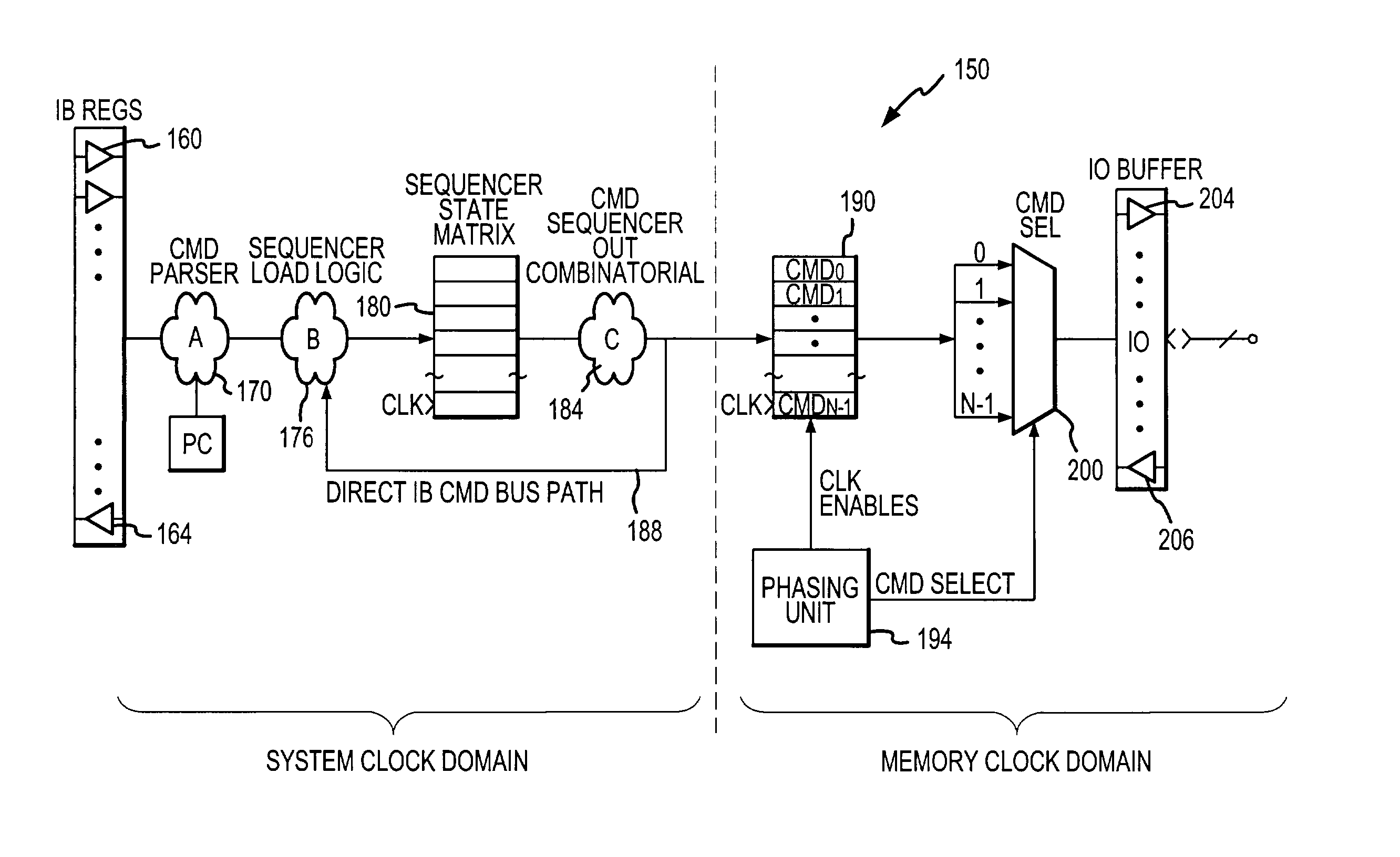
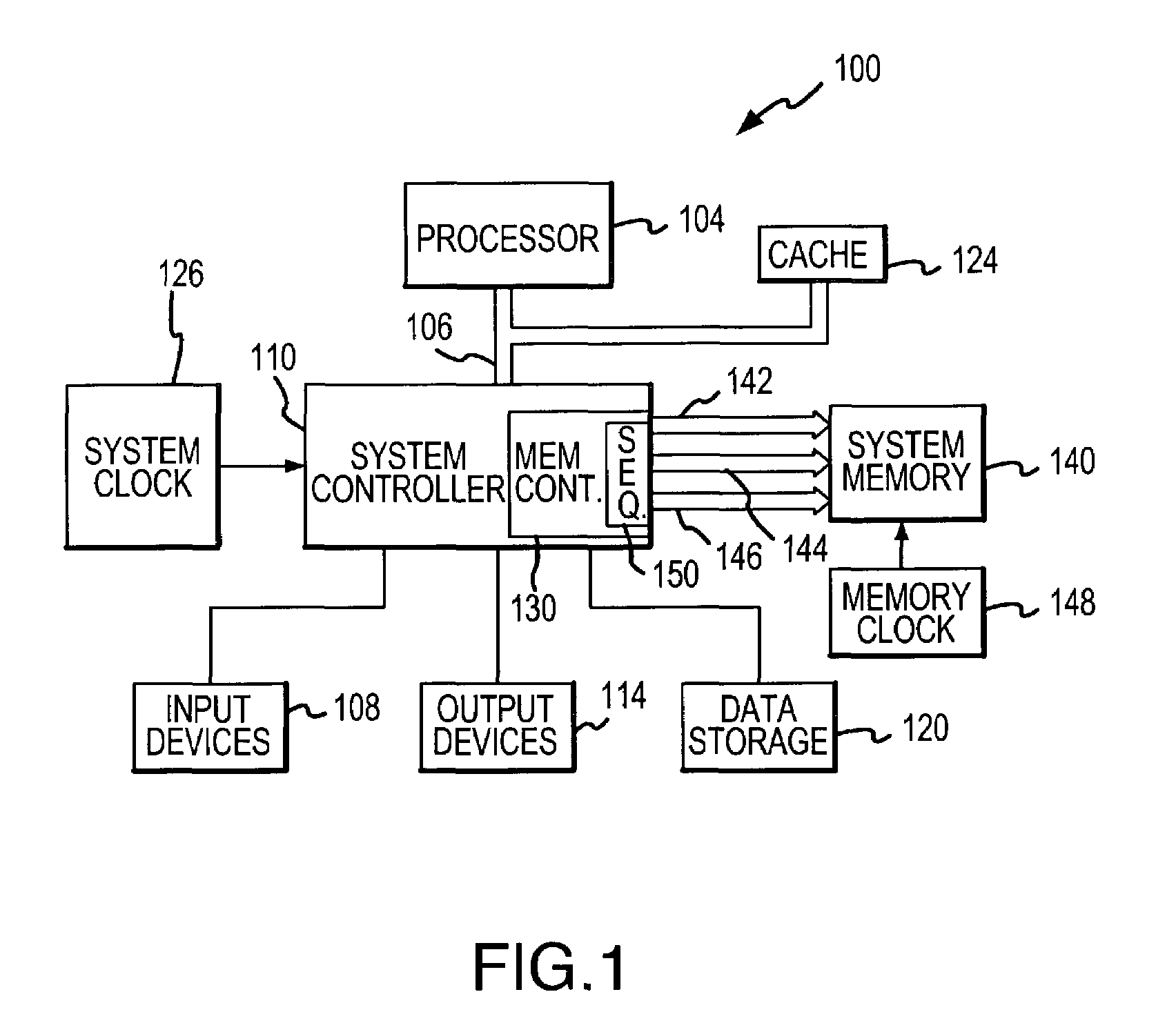
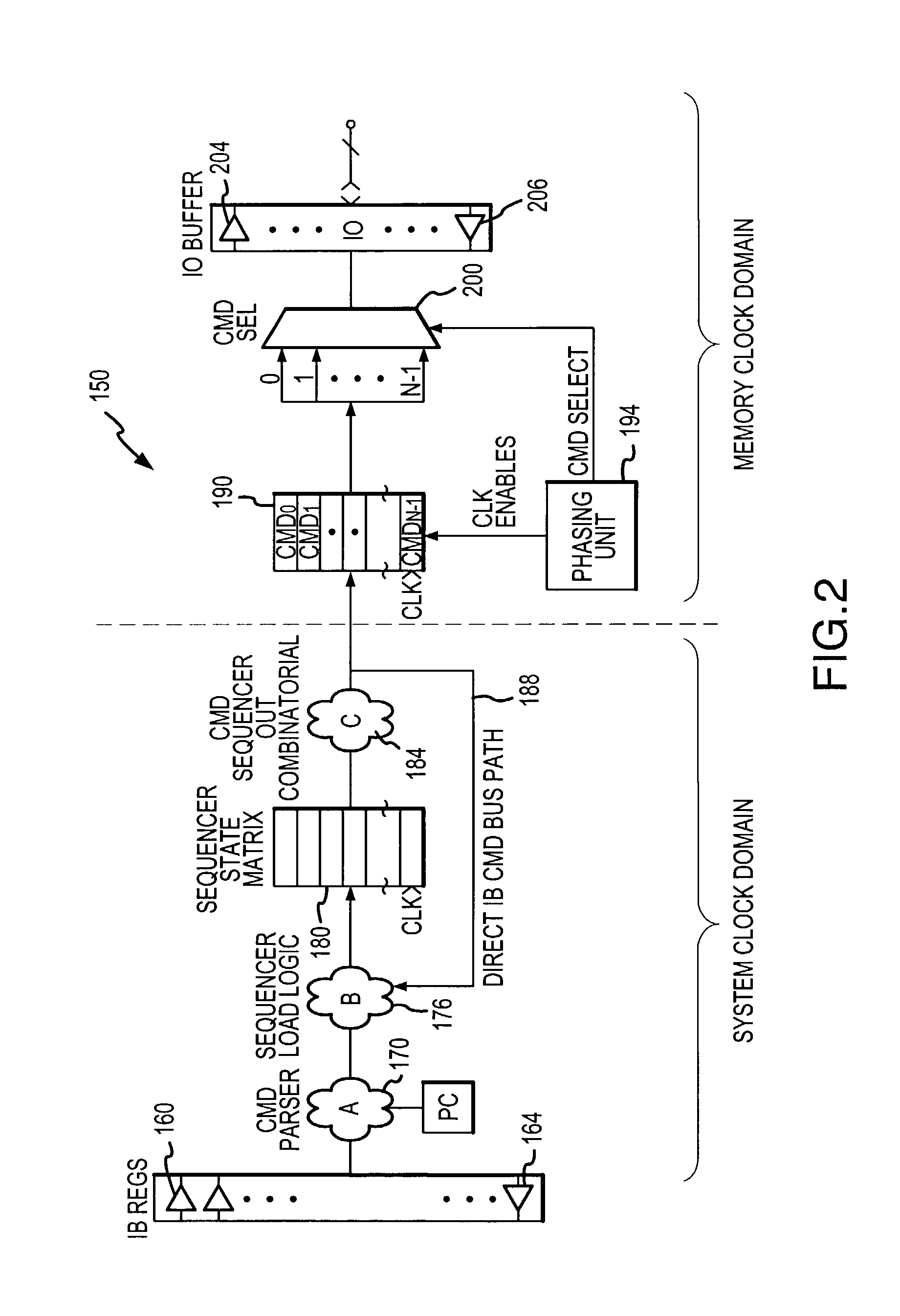
[0009]A computer system 100 according to one embodiment of the invention is shown in FIG. 1. The computer system 100 includes a processor 104 for performing various computing functions, such as executing specific software to perform specific calculations or tasks. The processor 104 includes a processor bus 106 that normally includes an address bus, a control bus, and a data bus. In addition, the computer system 100 includes one or more input devices 108, such as a keyboard or a mouse, coupled to the processor 104 through a system controller 110 to allow an operator to interface with the computer system 100. Typically, the computer system 100 also includes one or more output devices 114 coupled to the processor 104 through the system controller 110, such output devices typically being a printer or a video terminal. One or more data storage devices 120 are also typically coupled to the processor 104 through the system controller 110 to allow the processor 104 to store data or retrieve...


PUM


Abstract

A sequence state matrix has a plurality of time slots for storing a plurality of memory device signals. The memory device signals are loaded into the matrix by a sequencer load unit, which loads the memory device signals at locations in the matrix corresponding to the times that the signals will be coupled to a memory device. The sequencer load unit loads the signals into the matrix at a rate corresponding to a frequency of a system clock signal controlling the operation of the electronic system. A first in, first out (“FIFO”) buffer receives the memory device signals from the sequence state matrix at a rate corresponding to the frequency of the system clock signal. A command selector transfers the memory device signals from the FIFO buffer to the memory device at a rate corresponding to the frequency of a memory clock signal controlling the operation of the memory device.

Description

TECHNICAL FIELD[0001]This invention relates to memory devices, and more particularly to a system and method for interfacing a memory device to a system in which the system and memory device may operate at different clock speeds.BACKGROUND OF THE INVENTION[0002]Memory devices, such as dynamic random access memories (“DRAMs”) may operate either asynchronously or synchronously. When operating synchronously, the operation of the memory device is controlled by a clock signal, and the speed at which the memory device operates is thus determined by the frequency of the clock signal. The memory device may be interfaced with an electronic device, such as a computer system, that is also operated synchronously at a frequency determined by its own clock signal, known as the system clock signal. Generally, the frequency of the system clock signal is the same as the frequency of the memory clock signal. However, it is often possible for a memory device to operate at a higher speed than the speed ...

Claims


Application Information

Patent Timeline
IPC IPC(8): G06F12/00G06F13/00G06F13/16
CPCG06F13/1689
Inventor JEDDELOH, JOSEPH M.
Owner MICRON TECH INC
Why Eureka
Try Eureka