Method of manufacturing light-emitting diode device

a technology of light-emitting diodes and manufacturing methods, which is applied in the direction of semiconductor devices, basic electric elements, electrical appliances, etc., can solve the problems of low luminance of surface mountable led packages, deformation of packaging and transparent molding materials, and deformation of characteristic characteristics, so as to improve luminance characteristics and simple manufacturing process

Inactive Publication Date: 2006-01-10
SAMSUNG ELECTRONICS CO LTD
View PDF6 Cites 20 Cited by
  • Summary
  • Abstract
  • Description
  • Claims
  • Application Information

AI Technical Summary

Benefits of technology

[0014]Accordingly, the object of the present invention is to alleviate the problems encountered in the related art and to provide a method of manufacturing a light-emitting diode device,

Problems solved by technology

While the characteristics of such an LED device mainly depend on a compound semiconductor material used for the LED chip, they are further affected by a structure of the package for use in mounting the LED chip.
The surface mountable LED package suffers from low luminance due to a broad luminance distribution.
However, such an LED device is disadvantageous in terms of characteristic deterioration and decreased functions, resulting from defects of crystals caused by artificial growth in the compound semiconductor, serving as the emitting source.
Further, packaging and transparent molding materials may be degraded in characteristics thereof, t

Method used


Image

  • Method of manufacturing light-emitting diode device
  • Method of manufacturing light-emitting diode device
  • Method of manufacturing light-emitting diode device

Examples


Embodiment Construction

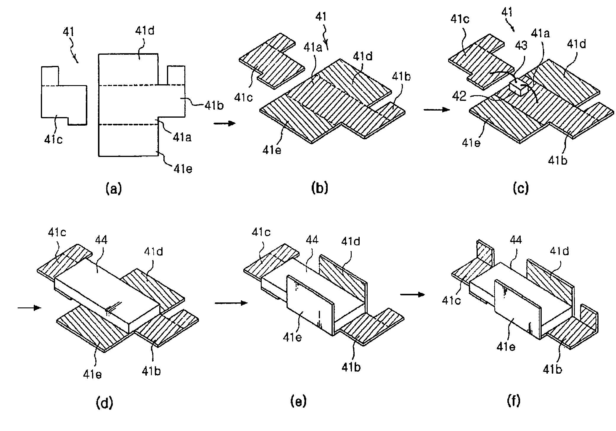
[0026]Based on the present invention, a method of manufacturing an LED device according to a mold type or a pre-mold type is provided, to easily and simply form reflective surfaces by use of a lead frame, in which a manufacturing method of a mold type LED device differs in procedures thereof from that of a pre-mold type LED device.

[0027]Referring to FIG. 4, there is sequentially shown a process of manufacturing the mold type LED device, according to a primary embodiment of the present invention.

[0028]The mold type LED device forms a package structure by a molding process directly without a pre-molding process, and is fabricated by the following procedures.

[0029]As shown in FIG. 4a, a lead frame 41 is formed for supporting an LED chip and forming electrodes for electric signal applications. As such, the lead frame 41 comprises a first pattern part 41a for use in mounting an LED chip thereon, a second pattern part 41b electrically connected to the first pattern part 41a to be used as ...


PUM


Abstract

A method of manufacturing a light-emitting diode (LED) device includes forming a lead frame having a first pattern part mounted with an LED chip, a second pattern part electrically connected to the first pattern part to be used as an electrode, a third pattern part spaced from the first pattern part to be electrically insulated from the first pattern part and used as another electrode, and a fourth pattern part and a fifth pattern part integrated with both sides of the first pattern part, forming a layer plated with a metal having high reflectivity on the fourth and fifth pattern parts, and upwardly folding the fourth and fifth pattern parts to be perpendicular to the first pattern part to form reflective surfaces.

Description

BACKGROUND OF THE INVENTION[0001]1. Field of the Invention[0002]The present invention relates, in general, to surface mountable light-emitting diode devices. More specifically, the present invention is directed to a method of manufacturing a light-emitting diode device, capable of simply forming reflective surfaces made of a metal material by use of a lead frame.[0003]2. Description of the Related Art[0004]As well known to those skilled in the art, a light-emitting diode (hereinafter, referred to as ‘LED’) composed of a compound semiconductor, such as GaAs, AlGaAs, GaN, InGaN or AlGaInP, as a light-emitting source, is a semiconductor device capable of emitting light of various colors.[0005]With great advances in semiconductor techniques, LED devices have recently been produced to have high luminance and quality characteristics, in place of commercially available LED products with low luminance. In addition, fabrication of blue and white diodes has been practically realized, whereby ...

Claims


Application Information

Patent Timeline
IPC IPC(8): H01L21/00H01L21/48H01L33/56H01L33/60H01L33/62
CPCH01L33/62H01L33/60H01L2924/0002H01L2924/00
Inventor YOON, JOON HO
Owner SAMSUNG ELECTRONICS CO LTD
Why Eureka
Try Eureka