Silicon nanoparticle field effect transistor and transistor memory device

a technology of transistors and nanoparticles, applied in the field of single electron technology transistors, can solve problems such as thermal fluctuations in the temperature operation of such devices

Inactive Publication Date: 2006-01-10
THE BOARD OF TRUSTEES OF THE UNIV OF ILLINOIS
View PDF21 Cites 52 Cited by
  • Summary
  • Abstract
  • Description
  • Claims
  • Application Information

AI Technical Summary

Benefits of technology

[0010]The transistor of the invention also forms the basis for a memory device. The devic

Problems solved by technology

A challenging problem for room temperature operati

Method used


Image

  • Silicon nanoparticle field effect transistor and transistor memory device
  • Silicon nanoparticle field effect transistor and transistor memory device
  • Silicon nanoparticle field effect transistor and transistor memory device

Examples


Embodiment Construction

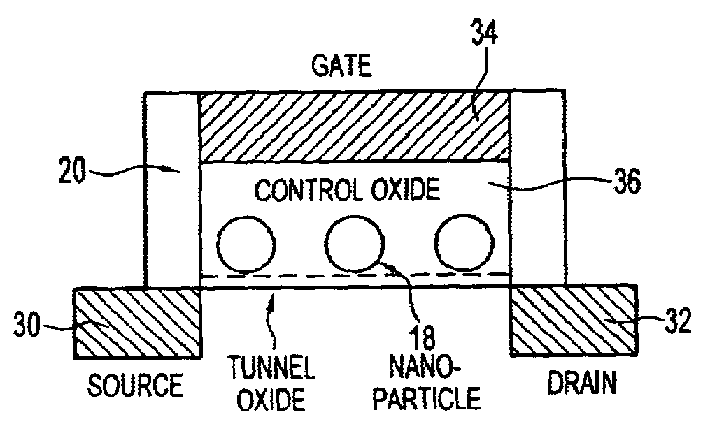
[0021]The present invention concerns single electron transistor devices which rely upon elemental silicon nanoparticles. The silicon nanoparticles provide a set of discrete levels for electron capture with energy spacing much larger than the thermal fluctuation energy.

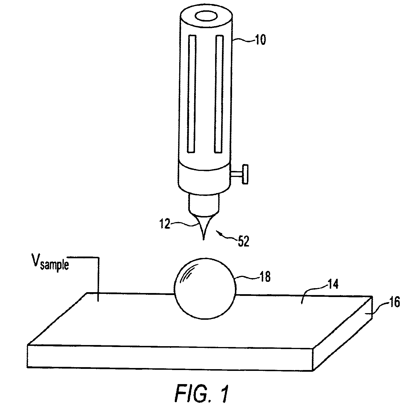
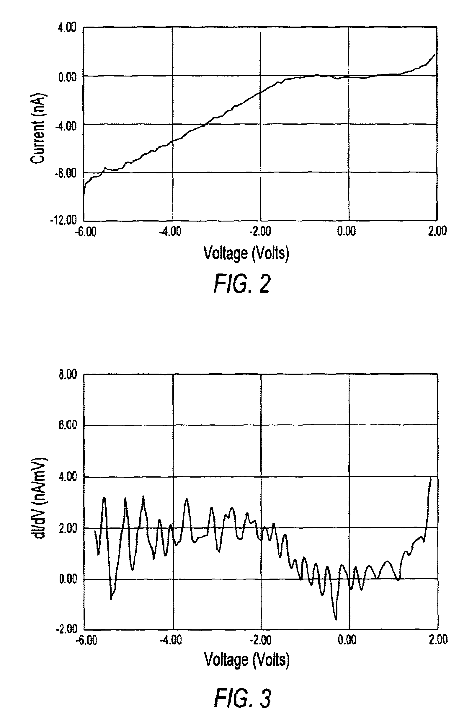
[0022]Silicon nanoparticles of diameter ˜1 nm, have a discrete set of states resulting from the quantum mechanical wave-like nature of electrons, capable of capturing / emitting single charge carriers, with an energy spacing on the order of 1 electron volt, and a discrete set of electric charging potential energy of 0.24 eV spacing. We demonstrated single electron transport through the particles at room temperature. The I-V spectra, taken using a scanning tunneling microscope, show single electron charging effects at a spacing of ˜0.26 eV. In addition, upon light irradiation, and superimposed on the charging resonances, near one hundred percent resolved single electron conductance resonance are observed with a spacing co...


PUM


Abstract

A silicon nanoparticle transistor and transistor memory device. The transistor of the invention has silicon nanoparticles, dimensioned on the order of 1 nm, in a gate area of a field effect transistor. The resulting transistor is a transistor in which single electron flow controls operation of the transistor. Room temperature operation is possible with the novel transistor structure by radiation assistance, with radiation being directed toward the silicon nanoparticles to create necessary holes in the quantum structure for the flow of an electron. The transistor of the invention also forms the basis for a memory device. The device is a flash memory device which will store electrical charge instead of magnetic effects.

Description

REFERENCE TO RELATED APPLICATION[0001]This application is a continuation-in-part application of prior application to Nayfeh et al., Ser. No. 09 / 426,204, now U.S. Pat. No. 6,597,496, issued Jul. 22, 2003, entitled SILICON NANOPARTICLE STIMULATED EMISSION DEVICES, filed on Oct. 25, 1999 now U.S. Pat. No. 6,597,496.FIELD OF THE INVENTION[0002]The present invention concerns transistors. More particularly, the invention concerns single electron technology transistors, being transistors in which one-by-one transport of electrons controls device operation.INCORPORATION BY REFERENCE OF COMMONLY OWNED RELATED APPLICATION[0003]A co-pending and commonly owned application to Nayfeh et al., Ser. No. 09 / 426,389, entitled SILICON NANOPARTICLES AND METHOD FOR PRODUCING THE SAME, filed on Oct. 22, 1999, is incorporated by reference herein.BACKGROUND OF THE INVENTION[0004]Transistors are the basic building block of electronic devices. The power of a transistor depends, in large part, on its switching...

Claims


Application Information

Patent Timeline
IPC IPC(8): H01L29/06
CPCB82Y10/00B82Y30/00H01L29/7888H01L29/42332H01L29/7883H01L21/28273H01L29/40114
Inventor NAYFEH, MUNIR H.THERRIEN, JOELBELMOIN, GENNADIY
Owner THE BOARD OF TRUSTEES OF THE UNIV OF ILLINOIS
Why Eureka
Try Eureka