Active matrix organic electroluminescence display device

a technology of organic electroluminescence and display device, which is applied in the direction of thermoelectric devices, semiconductor/solid-state device details, transistors, etc., can solve the problems of decaying the brightness of organic light-emitting diodes when given current, and achieve the effect of reducing leakage current, improving passivation layer structure, and maintaining stably

Active Publication Date: 2006-01-31
AU OPTRONICS CORP
View PDF4 Cites 21 Cited by
  • Summary
  • Abstract
  • Description
  • Claims
  • Application Information

AI Technical Summary

Benefits of technology

[0006]An object of the present invention is to provide an active matrix organic electroluminescence display device capable of maintaining the brightness of the organic light emitting diode. By improving the structure of the passivation layer of the thin film transistor to reduce the leakage current occurring in the TFT, the brightness of the organic light emitting diode can be stably maintained.

Problems solved by technology

However, in the current technology, the brightness of the organic light emitting diode decays when the given current is provided.

Method used


Image

  • Active matrix organic electroluminescence display device
  • Active matrix organic electroluminescence display device
  • Active matrix organic electroluminescence display device

Examples


first embodiment

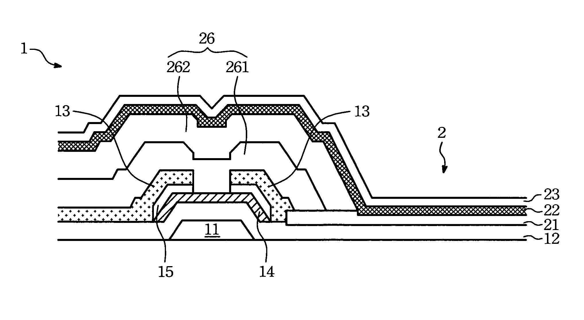
[0020]Refer to FIG. 5, which is a schematic side view of a structure of the passivation layer of the TFT of the AMOLED in accordance with this invention. A passivation layer 26 of a multi-layer structure is fabricated to enhance the current-leakage resistant ability of the passivation layer 26. For instance, at least two-layer SiNx is plated, each layer of which is in a 3000 Å thickness. Alternatively, one layer of the at least two-layer structure is made of SiNx and another layer is made of the other dielectric material. As shown in FIG. 5, the passivation layer 26 is composed by a two-layer structure 261, 262. The current-leakage resistant ability of the passivation layer 26 can be doubly enhanced by increasing the thickness of the dielectric layer of the passivation layer and increasing the interface between the dielectric layers because of multi-layer plating.

second embodiment

[0021]Furthermore, the surface of the passivation layer can also be treated by thermal oxidation in this invention to enhance the current-leakage resistant ability of the passivation layer. FIG. 6 is a schematic side view of a structure of the passivation layer of the TFT of the AMOLED in accordance with this invention. For instance, after a SiNx passivation layer 36 is plated, the SiNx layer is in a thermal oxidation treatment and SiON is formed on the surface 36′ of the passivation layer 36 to enhance the current-leakage resistant ability of the passivation layer.

third embodiment

[0022]In addition, FIG. 7 is a schematic side view of a structure of the passivation layer of the TFT of the AMOLED in accordance with this invention. A high dielectric material such as SiO2 can be used to fabricate a passivation layer 46 to enhance the current-leakage resistant ability of the passivation layer.


PUM


Abstract

An active matrix organic electroluminescence display device capable of maintaining the brightness of the organic light emitting diode. The active matrix organic electroluminescence display device comprises a thin film transistor and an organic light emitting diode. By improving the structure of the passivation layer of the thin film transistor to reduce the leakage current occurring in the TFT, the brightness of the organic light emitting diode can be stably maintained.

Description

FIELD OF THE INVENTION[0001]The present invention relates to an organic electroluminescence display device and, more specifically, to a structure of an active matrix organic electroluminescence display device for reducing the leakage current occurring in the thin-film transistor so as to maintain the brightness of the organic light emitting diode.BACKGROUND OF THE INVENTION[0002]Owing to high brightness, fast response speed, light weight, thin and small features, full color, no viewing angle differences, no need for an LCD back-light board and low electrical consumption, an organic light emitting diode display or organic electroluminescence display (OLED) takes the lead to substitute a twist nematic (TN) or a super twist nematic (STN) liquid crystal display. Further, it substitutes for a small-sized thin-film transistor (TFT) LCD to become a new display material of fabricating portable information products, cell phones, personal digital assistant (PDA) and notebook.[0003]The organic...

Claims


Application Information

Patent Timeline
Patent Type & Authority Patents(United States)
IPC IPC(8): H01L35/24H01L27/32
CPCH01L27/1248H01L27/3258H01L27/3246H01L27/3248H10K59/123H10K59/124H10K59/122
Inventor HUANG, WEI-PANG
Owner AU OPTRONICS CORP
Why Eureka
Try Eureka