Piezoelectric/electrostrictive device and method of manufacturing same

Inactive Publication Date: 2006-01-31
NGK INSULATORS LTD
View PDF19 Cites 40 Cited by
  • Summary
  • Abstract
  • Description
  • Claims
  • Application Information

AI Technical Summary

Benefits of technology

[0020]The present invention has been made taking the foregoing problems into consideration, an object of which is to provide a piezoelectric / electrostrictive device which makes it possible to increase the occupied area of a conductive portion in one electrode layer, which increases the driving force, which improves the yield, and which is easily controllable, and a method for producing the same.
[0021]Another object of the present invention is to provide a piezoelectric / electrostrictive device which makes it possible to effectively reduce the volume of a piezoelectric / electrostrictive element itself to decrease the resistance on the displacement action and which makes it possible to further increase the driving force (increase the displacement amount) in addition to the requirements described above, and a method for producing the same.
[0022]Still another object of the present invention is to provide a piezoelectric / electrostrictive device which makes it possible to prevent a piezoelectric / electrostrictive element formed on a ceramic substrate from exfoliation, reduce the number of steps in relation to the production of the piezoelectric / electrostrictive device, and improve the throughput and which also makes it possible to avoid the deterioration of function of the piezoelectric / electrostrictive device, and a method for producing the same.

Problems solved by technology

As a result, a lot of unnecessary pores appear in the wiring pattern and pores having large opening areas appear to decrease the portion (conductive portion) which actually functions as the electrode layer.
This results in decreasing yield of the devices.
A problem occurs in that such a device is difficult to be used (difficult to be controlled).
Further, the adhesive force is weak between the wiring pattern and the piezoelectric / electrostrictive layer.
That is, it is difficult to join constitutive materials of the ceramic substrate and constitutive materials of the piezoelectric / electrostrictive layer.
(1) The function as the piezoelectric / electrostrictive device is deteriorated.

Method used


Image

  • Piezoelectric/electrostrictive device and method of manufacturing same
  • Piezoelectric/electrostrictive device and method of manufacturing same
  • Piezoelectric/electrostrictive device and method of manufacturing same

Examples


Embodiment Construction

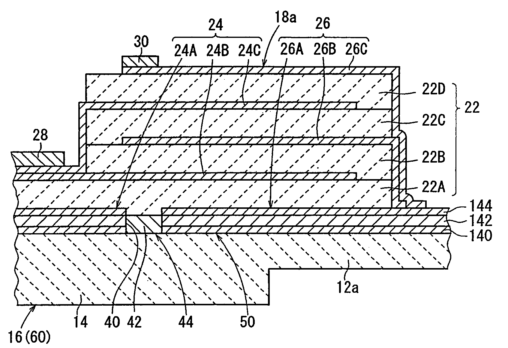
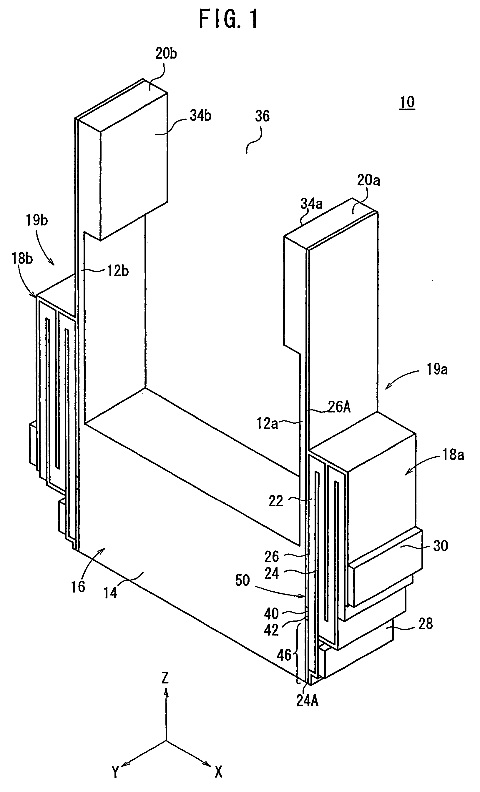
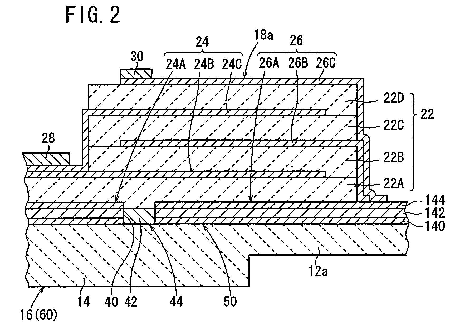
[0093]Embodiments of the piezoelectric / electrostrictive device according to the present invention and the method for producing the same will be described below with reference to FIGS. 1 to 24.

[0094]A piezoelectric / electrostrictive device 10 according to the present embodiment is a device or element which includes a concept that the electric energy and the mechanical energy are mutually convertible through a piezoelectric / electrostrictive element. Therefore, the piezoelectric / electrostrictive device 10 is preferably an active element such as a variety of actuators and vibrators, and is more preferably a displacement element for displacing on the basis of the inverse piezoelectric effect and the electrostrictive effect. The piezoelectric / electrostrictive device 10 is also preferably a passive element such as an acceleration sensor element and a shock sensor element.

[0095]As shown in FIG. 1, the piezoelectric / electrostrictive device 10 according to the present embodiment comprises a ce...


PUM


Abstract

A pair of opposing thin plate sections, movable sections, and fixed sections for supporting the thin plate sections and the movable sections are provided on a ceramic substrate. After a wiring pattern and a gap or an insulating layer of cermet layer for filling the gap are formed on a ceramic substrate, these are sintered. After that, piezoelectric / electrostrictive layers and cermet electrode layers including a piezoelectric / electrostrictive material and a conductive material are alternately stacked in a comb like structure on the ceramic substrate. Accordingly, a piezoelectric / electrostrictive device having the piezoelectric / electrostrictive element in multilayer structure is obtained.

Description

CROSS REFERENCE TO RELATED APPLICATIONS[0001]This application is a division of U.S. application Ser. No. 10 / 341,543, filed Jan. 13, 2003 now U.S. Pat. No. 6,809,459, the entirety of which is incorporated herein by reference.[0002]This application also claims the benefit of Japanese Application No. 2002-005289, filed Jan. 11, 2002, the entirety of which is incorporated herein by reference.BACKGROUND OF THE INVENTION[0003]1. Field of the Invention[0004]The present invention relates to a piezoelectric / electrostrictive device comprising a ceramic substrate and at least a piezoelectric / electrostrictive element stacked on the ceramic substrate by means of a film formation method, and more particularly to a piezoelectric / electrostrictive device comprising a plurality of piezoelectric / electrostrictive layers and a plurality of electrode layers including a piezoelectric / electrostrictive material stacked alternately in a comb like structure on a ceramic substrate and to a method for producing...

Claims


Application Information

Patent Timeline
IPC IPC(8): H01L41/04H01L41/047H01L41/083H01L41/09H01L41/273H01L41/297
CPCH01L41/0477H01L41/273H01L41/0946H01L41/0831H01L41/297H10N30/877H10N30/501H10N30/2043H10N30/053H10N30/067
Inventor IKEDA, KOJITAKAHASHI, FUMITAKESHIBATA, KAZUYOSHIITOH, HARUHIKO
Owner NGK INSULATORS LTD
Why Eureka
Try Eureka