Semiconductor memory device with built-in self test circuit operating at high rate

a memory device and self-testing technology, applied in the direction of error detection/correction, semiconductor/solid-state device testing/measurement, instruments, etc., can solve the problems of high probability of defect, high cost of apparatus, interference of data between adjacent cells, etc., to increase the storage capacity of semiconductor memory devices and reduce the investment in testing equipmen

Inactive Publication Date: 2006-01-31
RENESAS ELECTRONICS CORP +1
View PDF10 Cites 28 Cited by
  • Summary
  • Abstract
  • Description
  • Claims
  • Application Information

AI Technical Summary

Benefits of technology

[0016]An object of the present invention is to provide a semiconductor memory device that can suppress investment in equipment for testing with respect to increase in the storage capacity of a semiconductor memory device.
[0017]Another object of the present invention is to provide a semiconductor memory device that can carry out testing more flexibly.
[0018]A further object of the present invention is to provide a semiconductor memory device that can carry out testing by a desired pattern after fabrication.

Problems solved by technology

The possibility is high of a defect being caused by dust and the like during the fabrication process.
Also, the interference of data between adjacent cells cannot be ignored in accordance with the microminiaturization of the memories.
The ATE is an expensive apparatus.
Since the number of memory cells to be subjected to testing increases, the time required for testing will take longer if the above-described method is employed.
Therefore, the time required for testing also increases significantly.
As a result, the effect on data caused by interference between input / output data has increased.
However, such testing is difficult with the above-described degeneration test.
Thus, there was a problem that the required chip area becomes larger.
The case where an ROM is employed cannot cope with such a problem.

Method used


Image

  • Semiconductor memory device with built-in self test circuit operating at high rate
  • Semiconductor memory device with built-in self test circuit operating at high rate
  • Semiconductor memory device with built-in self test circuit operating at high rate

Examples


first embodiment

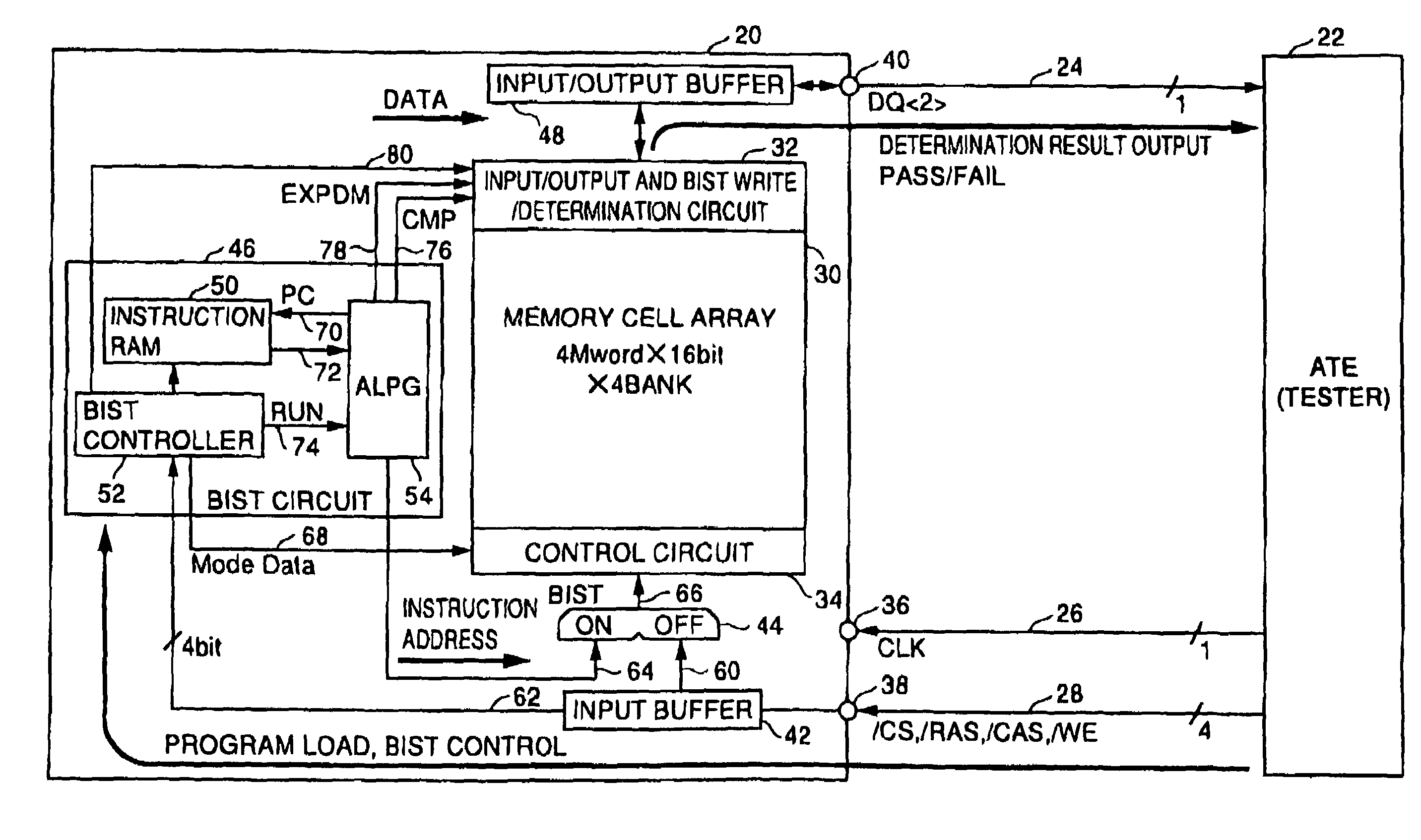
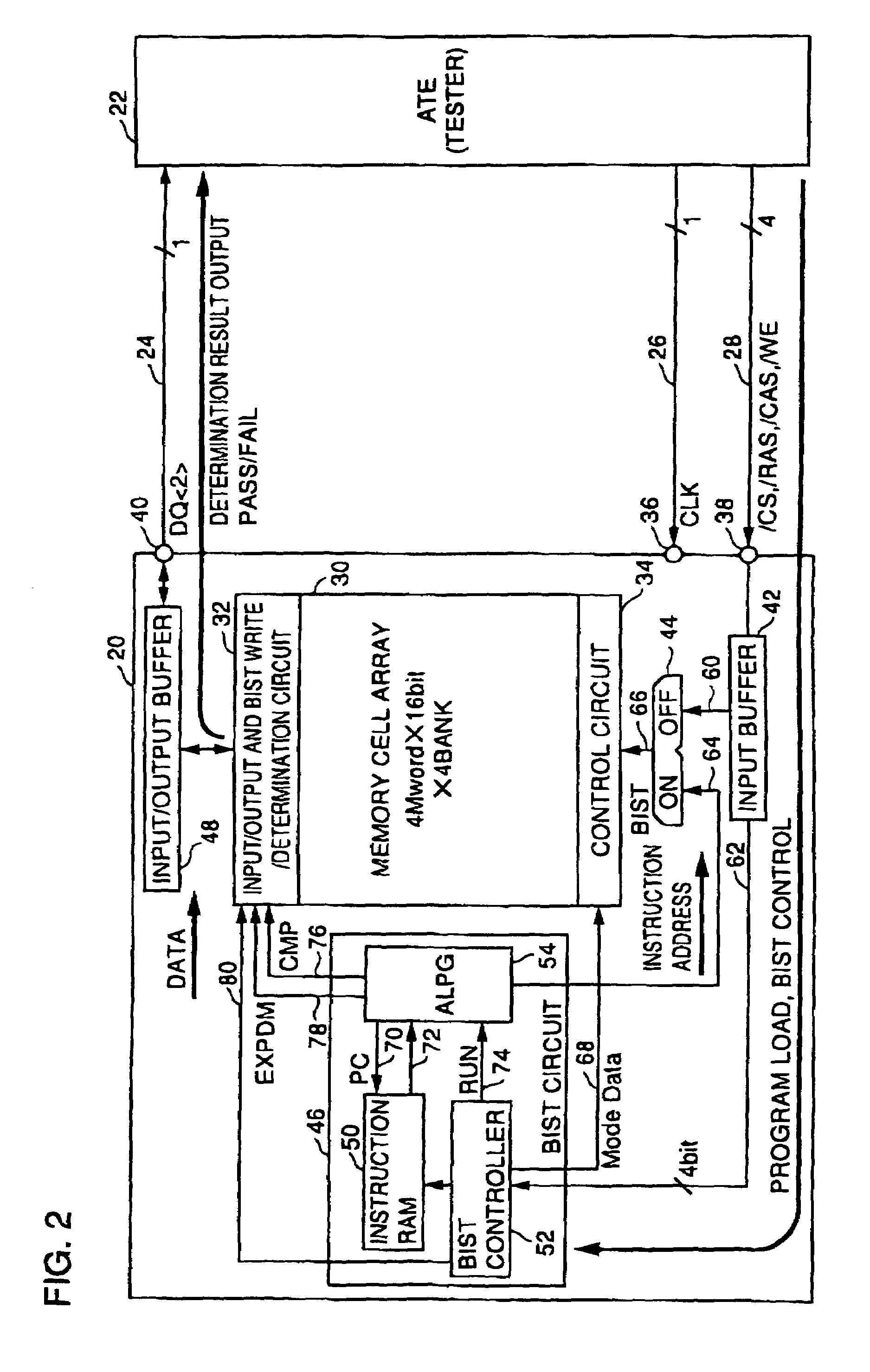
[0051]Referring to FIG. 2, a memory 20 with a built-in self test circuit according to the present invention is connected to a tester 22 through a tester 22 input / output pin 40 and an input / output line 24, a clock input pin 36 and a clock signal line 26, and four input pins 38 and input lines 28.

[0052]Memory 20 with a built-in self test circuit includes an input buffer 42, a built-in self test (BIST) circuit 46, a memory cell array 30, a control circuit 34 to control the operation of memory cell array 30, an input / output and BIST write / determination circuit 32 providing data to / from memory cell array 30 and input / output buffer 48 and having the function of determining the result of the self test, and a multiplexer 44 selecting and providing to output 66 to apply to control circuit 34 either the command / address applied from built-in self test (BIST) circuit 46 via a command / address line 64 or a control signal applied via input buffer 42 according to whether in a self test operation or...

second embodiment

[0096]The apparatus of the second embodiment allows testing to be carried out using a relatively economic ATE. Since a test pattern can be generated according to the program stored in instruction RAM 50 and the program stored in instruction RAM 50 can be applied to memory 180 with a built-in self test circuit from tester 182 via input line 28 and input pin 38 by ALPG 54, testing can be carried out readily with the required test pattern even after fabrication of a product. Testing can be carried out flexibly.

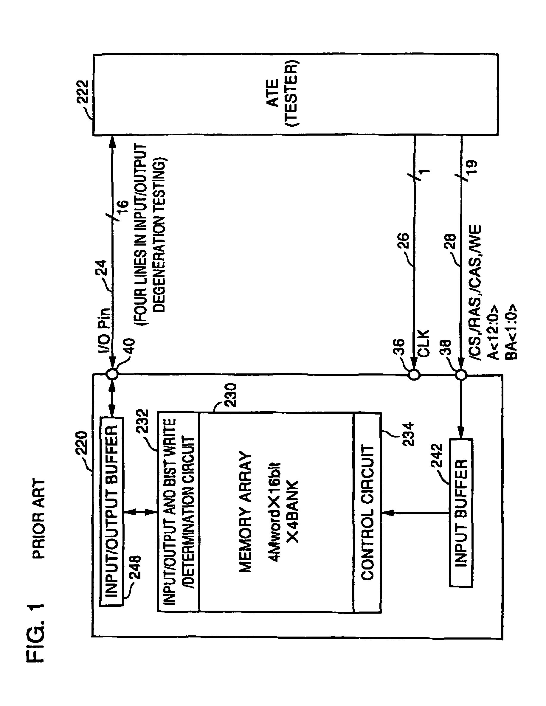
[0097]In the apparatus of the second embodiment, the total number of pins required for testing is 9 (four for input line 28, one for clock signal line 26 and four for input / output line 24 by degeneration). It is appreciated that the number of pins required for testing is reduced significantly in comparison to the conventional case shown in FIG. 1 where 24 pins were required even when degenerated.

[0098]The data read out from memory cell array 30 is output to tester 182 via input / o...


PUM


Abstract

A semiconductor memory device with a built-in self test circuit includes a semiconductor substrate, a memory cell array formed on the semiconductor substrate, an input buffer provided on the semiconductor substrate to receive externally applied data, a test circuit coupled to the memory cell array and the input buffer on the semiconductor substrate to store a program received through the input buffer to generate test data of the memory cell array according to the stored program to carry out testing of the memory cell array, and a select circuit selectively applying to the memory cell array test data applied from the test circuit and data applied from the input buffer depending upon a test operation and a normal operation.

Description

BACKGROUND OF THE INVENTION[0001]1. Field of the Invention[0002]The present invention relates to semiconductor memory devices, and more particularly to a semiconductor memory device with a built-in self test circuit (referred to as “BIST circuit” hereinafter).[0003]2. Description of the Background Art[0004]A semiconductor memory device includes a memory cell array with a plurality of memory cells. In accordance with microminiaturization of semiconductor memory devices, the size of each memory cell becomes smaller. The possibility is high of a defect being caused by dust and the like during the fabrication process. Also, the interference of data between adjacent cells cannot be ignored in accordance with the microminiaturization of the memories. It is therefore necessary to test the circuit including the memory cells prior to shipment of a semiconductor memory device as a product.[0005]Conventionally, a memory tester (auto test equipment; referred to as “ATE” hereinafter) is used to ...

Claims


Application Information

Patent Timeline
Patent Type & Authority Patents(United States)
IPC IPC(8): G01R31/28G06F11/00G06F11/22G11C11/401G11C29/00G11C29/12G11C29/16G11C29/36H01L21/66
CPCG11C29/16G11C29/36G11C2029/3602
Inventor TANIZAKI, TETSUSHISUGIURA, KAZUSHINAKAJIMA, MASAMI
Owner RENESAS ELECTRONICS CORP
Why Eureka
Try Eureka