Connector and contact wafer

a technology of contact wafer and connector, which is applied in the direction of connection contact material, fixed connection, coupling device connection, etc., can solve the problems of unreliable soldering and reliability of connector, and achieve the effect of improving the soldering speed of a connector to the circuit board, reducing thermal stress on other components, and improving the solderability of the circuit board

Inactive Publication Date: 2006-02-14
PERLOS OY
View PDF7 Cites 9 Cited by
  • Summary
  • Abstract
  • Description
  • Claims
  • Application Information

AI Technical Summary

Benefits of technology

[0012]An advantage of the invention is that when contact pins are soldered to the circuit board, hot air flows through the channel to the lowest contact pins and thus the temperature of these contact pins rises faster, which considerably improves their solderability to the circuit board compared to the prior art. Soldering of a connector to the circuit board becomes faster while the thermal stress on other components decreases. All in all, the costs of the soldering process decrease. Furthermore, less material is needed for the wafer body, which reduces the material costs.

Problems solved by technology

Soldering of connectors and contact pieces of the prior art to a circuit board involves the following problems: the bodies of wafers attached next to one another limit access of hot air to the lowest contact pins of the wafer.
In that case the temperature of the lowest contact pins and the surfaces to be soldered to the pins is lower than that of the other surfaces to be soldered and thus their soldering is unreliable.
This is naturally a problem in respect of the reliability of the connector.

Method used


Image

  • Connector and contact wafer
  • Connector and contact wafer
  • Connector and contact wafer

Examples


second embodiment

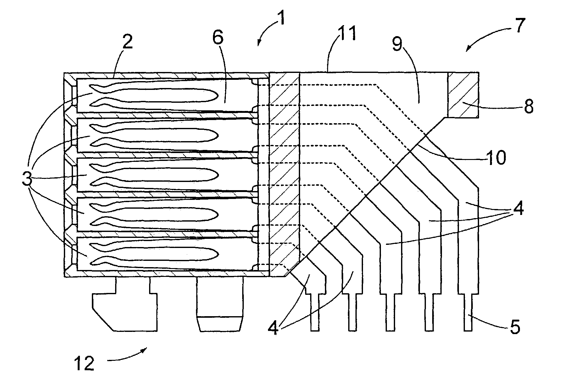
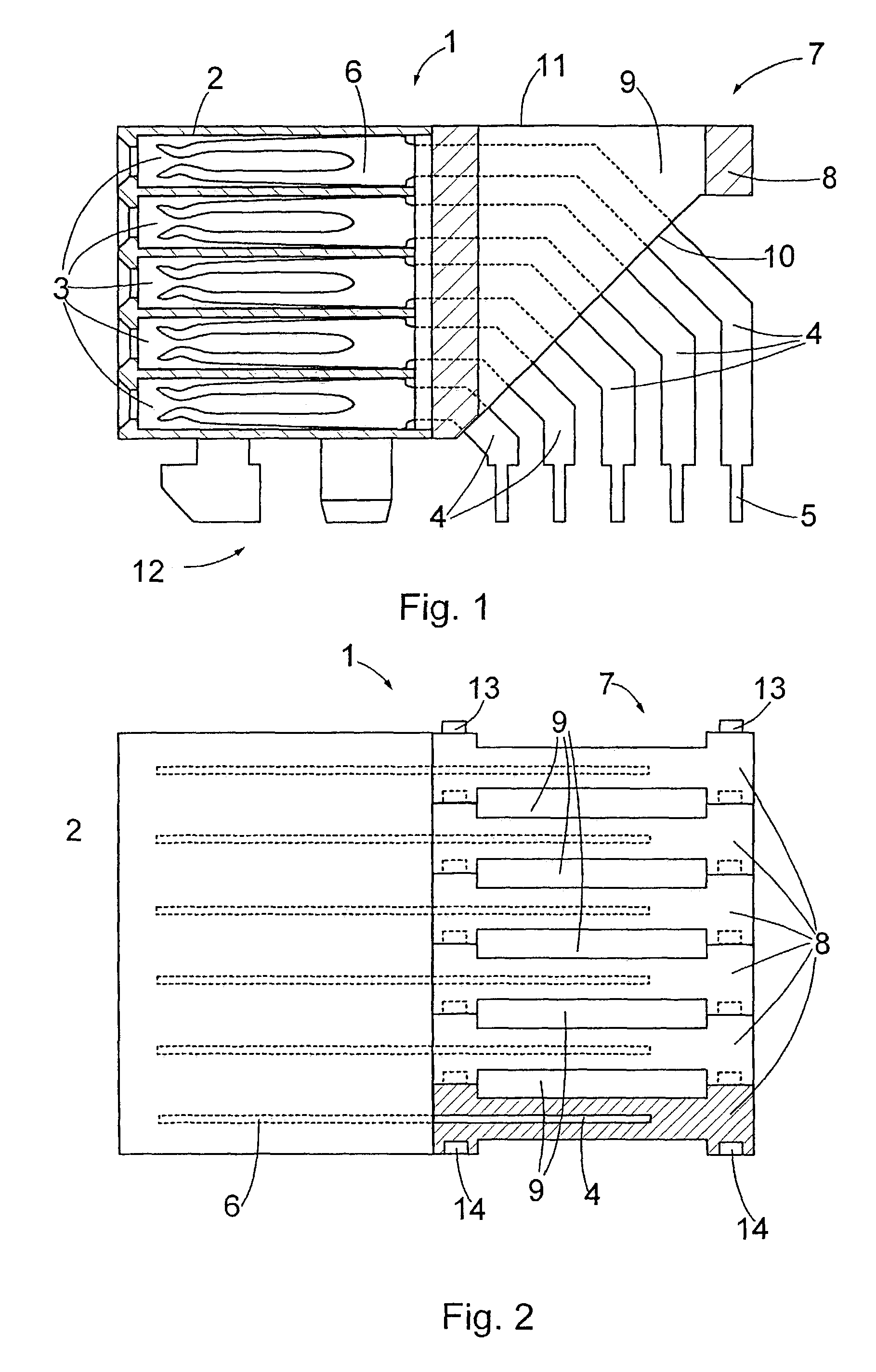
[0026]FIG. 3 is a schematic top view of the contact wafer attached to the connector body 2. To simplify the illustration, the connector body 2 is shown by a broken line in FIG. 3. The connector 1 comprises three wafers 7 arranged in parallel in the connector body 2. One side of the wafer body 8 is provided with a groove and each channel 9 is formed from the space defined by this groove and the body 8 of the other wafer arranged on the side of the groove. The channel 9 extends from the upper surface of the wafer body 8 to the lower surface and functions in the same way as described in connection with FIGS. 1 and 2.

third embodiment

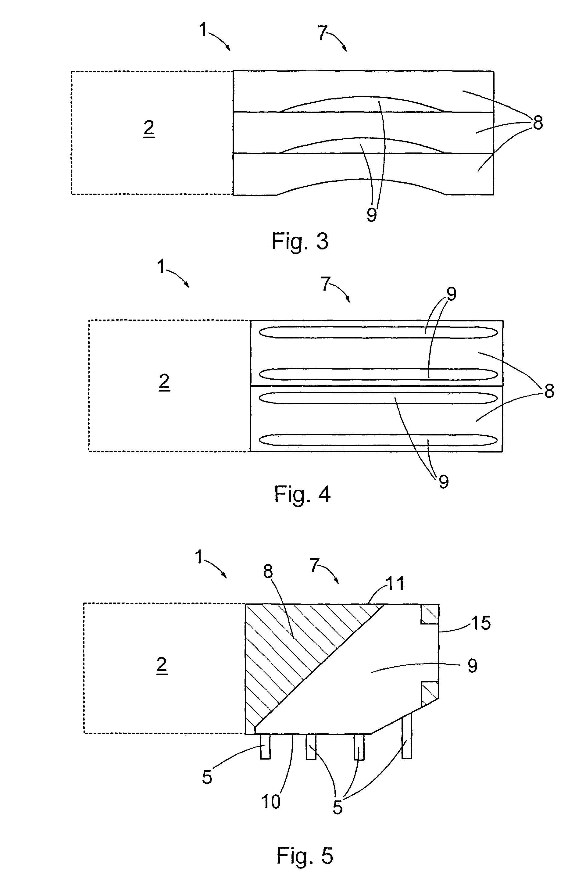
[0027]FIG. 4 is a schematic top view of the contact wafer attached to the connector body 2. To simplify the illustration, the connector body 2 is shown by a broken line in FIG. 4. The connector 1 comprises two wafers 7 which are arranged in parallel in the connector body 2. Now a single channel 9 is not formed between the body 8 of two wafers but the whole channel is arranged inside the body 8 of one and the same wafer, in other words, the shape of the body 8 of one wafer defines the shape of the channel 9. In the embodiment shown in FIG. 4 the body 8 of each wafer includes two channels 9 but the number of channels may naturally vary. The channels 9 extend through the body 8 of the wafer up to its lower surface.

fourth embodiment

[0028]FIG. 5 is a cross-sectional schematic side view of the contact wafer attached to the connector body 2. To simplify the illustration, the connector body 2 is shown by a broken line. One end of the channel 9 extends to the lower surface of the wafer body 8 and the other end partly to the upper surface and partly to the rear side, i.e. to the side away from the connector body 2. The channel 9 can also be shaped in various other ways, provided that it extends to the lower surface of the wafer body 8 and increases air circulation near the contact pins 5.

[0029]The drawings and the related description are only intended to illustrate the inventive concept. The details of the invention may vary within the scope of the claims. Thus the number of contacts in the wafer 7 and the number of wafers 7 in the connector 1 may differ from those shown in the figures. There does not need to be a channel 9 in each contact wafer 7 or between each two wafers 7. In the embodiment shown in FIG. 4 the t...


PUM


Abstract

A connector and a contact wafer. The connector (1) comprises contacts one on top of another and in parallel and the wafer body (8) comprises at least one channel (9) which is arranged between contacts (4) arranged in parallel and extends to the lower surface of the wafer body (8).

Description

CROSS REFERENCE TO RELATED APPLICATIONS[0001]This application is a Continuation of International Application PCT / FI02 / 00102 filed Feb. 11, 2002, which designated the U.S. and was published under PCT Article 21(2) in English.FIELD OF THE INVENTION[0002]The invention relates to a connector which comprises a connector body, contacts, which are arranged both one on top of another and parallel with one another partly inside the body, at least one wafer to which the contacts arranged one on top of another are attached and which comprises a wafer body.[0003]The invention further relates to a contact wafer which comprises a wafer body, at least two contacts which are arranged one on top of another, the wafer being arrangeable parallel with at least one other wafer in the connector body.BACKGROUND OF THE INVENTION[0004]The connectors concerned are used particularly for transmitting signals and electric current between circuit boards or generally in applications which require fast data transm...

Claims


Application Information

Patent Timeline
Patent Type & Authority Patents(United States)
IPC IPC(8): H01R13/502H01R12/50H01R13/514H05K3/34
CPCH01R23/6873H01R13/514H05K3/3447H01R23/7073H01R12/724H01R13/6586H01R12/00
Inventor VARIS, ARVO
Owner PERLOS OY
Why Eureka
Try Eureka