Semiconductor device and method for manufacturing the same, circuit board, electronic apparatus, and semiconductor device manufacturing apparatus
a semiconductor device and manufacturing method technology, applied in the direction of semiconductor devices, semiconductor/solid-state device details, electrical devices, etc., can solve the problems of increasing the manufacturing cost of semiconductor manufacturing devices, and achieve the effect of increasing the efficiency of semiconductor device manufacturing
- Summary
- Abstract
- Description
- Claims
- Application Information
AI Technical Summary
Benefits of technology
Problems solved by technology
Method used
Image

Examples
first embodiment
[0076][First Embodiment]
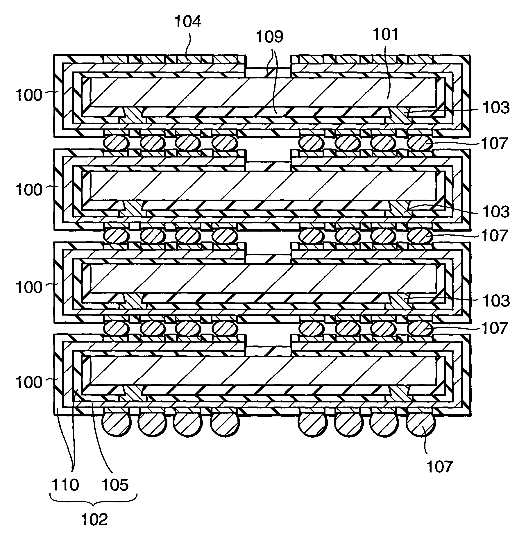
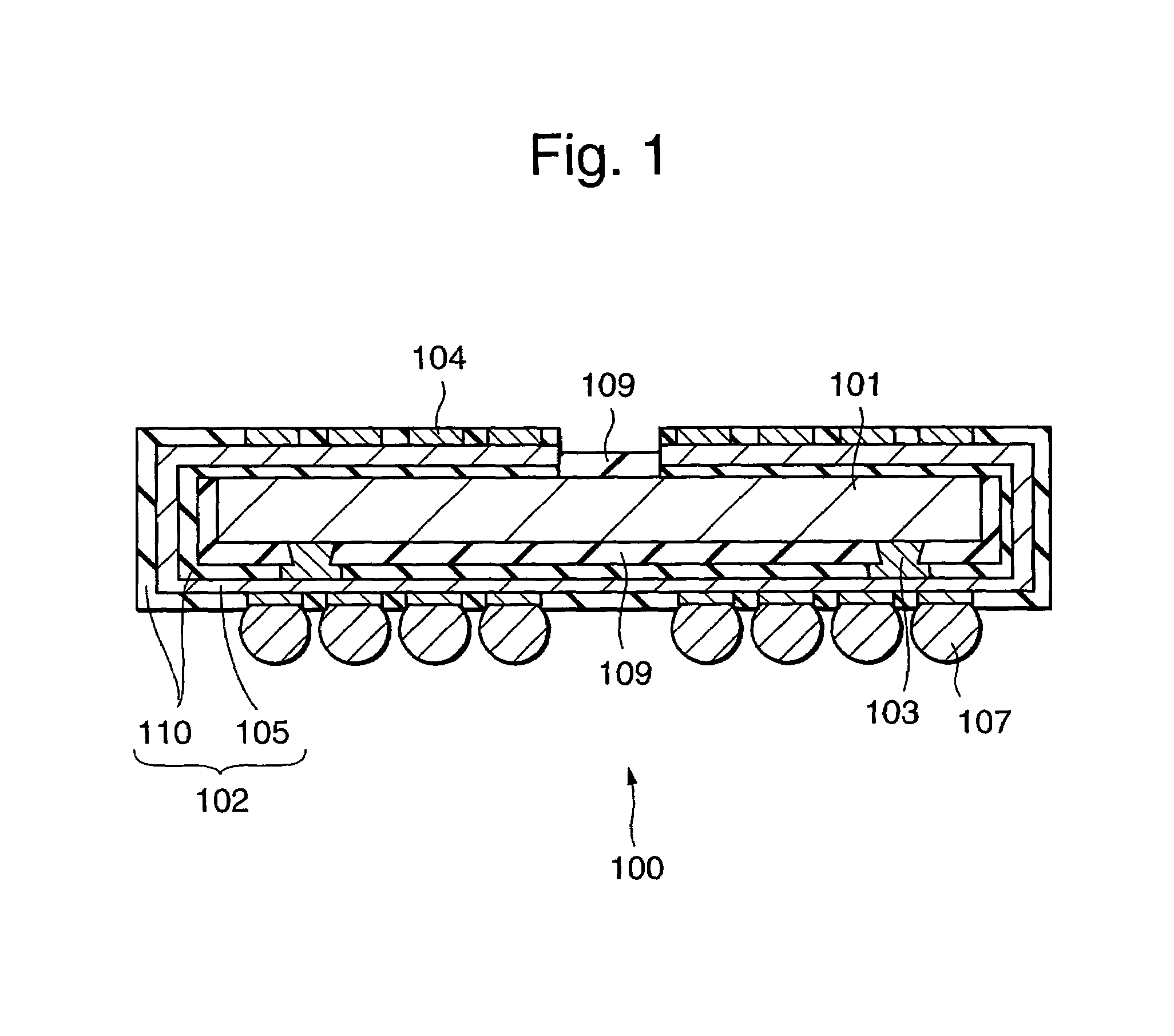
[0077]FIG. 9 is a sectional view of a semiconductor device according to a first embodiment of the present invention. FIGS. 10 through 13 are sectional views showing a method of manufacturing the semiconductor device according to the first embodiment. FIGS. 14 through 16 are sectional views showing another method of manufacturing the semiconductor device according to the first embodiment.
[0078]In the semiconductor device according to the first embodiment, a flat plate 6 is provided between the side facing the solder bump of a semiconductor chip 1 as shown in FIG. 9. The contour in plan view of the flat plate 6 is substantially the same size as that of the semiconductor chip 1. A flexible interposer substrate 11 covers the semiconductor chip 1 and the flat plate 6 by running along the entire circumference. The flexible interposer substrate 11 is composed of thermoplastic resin 2 placed on the semiconductor chip 1 side, insulating resin 3 that is thermoplastic r...
second embodiment
[0089][Second Embodiment]
[0090]FIG. 17 is a sectional view of the semiconductor device according to the second embodiment of the present invention. The semiconductor device of the second embodiment is different from the first embodiment in that a non-adhesive agent 18 is applied to the side surface of the semiconductor chip 1. Element corresponding to those described above with respect to the first embodiment are identified with the same reference numerals and a detailed description thereof will be omitted for the sake of brevity.
[0091]A method of manufacturing the semiconductor device according to this embodiment is similar to the method of manufacturing the semiconductor device according to the first embodiment. Prior to bonding the flexible interposer substrate 11 to the circumference of the semiconductor chip 1, the non-adhesive agent 18 is applied to the side surface of the semiconductor chip 1. The non-adhesive agent 18 is formed of, for example, fluorocarbon resin such as pol...
third embodiment
[0094][Third Embodiment]
[0095]FIG. 18 is a sectional view of the semiconductor device according to a third embodiment of the present invention. The semiconductor device of the third embodiment is different from the first embodiment in the contour in plan view of the flat plate 6 is smaller than that of the semiconductor chip 1. The semiconductor device according to this embodiment is manufactured by using a flat plate 6 whose contour in plan view is smaller than that of the semiconductor chip 1, and by the same method that is employed in the manufacturing method of the first embodiment.
[0096]In the third embodiment, the flat plate 6 which is in contact with but not fixed by adhesion to the semiconductor chip 1 and which is bonded to the flexible interposer substrate 11 has a contour in plan view that is smaller in size than the flat plate 6 of the first embodiment. Therefore, the flexible interposer substrate 11 is affected less by thermal expansion and cold shrinkage which are due ...
PUM
 Abstract
Description
Claims
Application Information
 - R&D
- Intellectual Property
- Life Sciences
- Materials
- Tech Scout
- Unparalleled Data Quality
- Higher Quality Content
- 60% Fewer Hallucinations
Browse by: Latest US Patents, China's latest patents, Technical Efficacy Thesaurus, Application Domain, Technology Topic, Popular Technical Reports.
© 2025 PatSnap. All rights reserved.Legal|Privacy policy|Modern Slavery Act Transparency Statement|Sitemap|About US| Contact US: help@patsnap.com