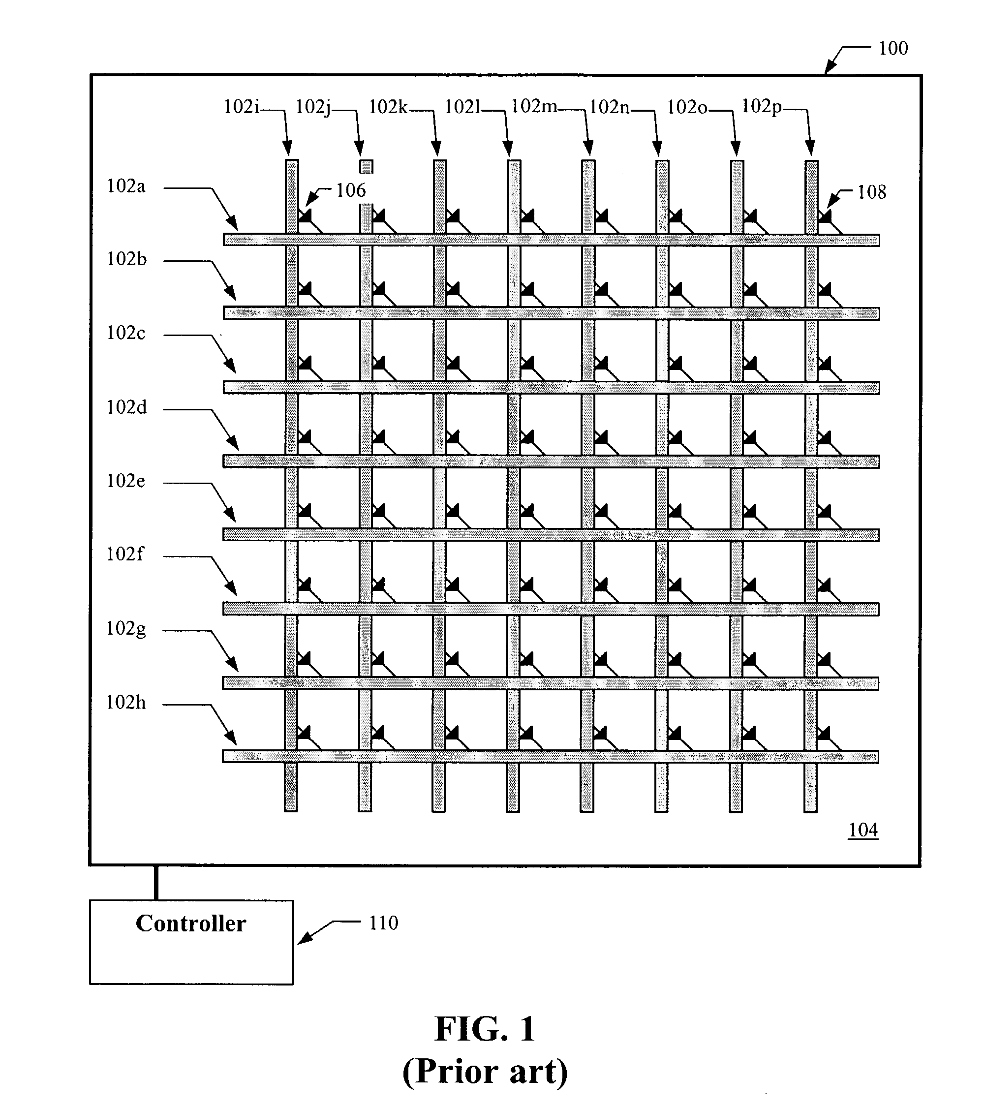
Check patentability & draft patents in minutes with Patsnap Eureka AI!

Switch matrix

a switch matrix and matrix technology, applied in the field of electronic switching, can solve the problems of high fabrication cost, increased insertion loss, and relatively expensive gaas substrates that are typically used in switch matrixes to minimize signal loss, so as to reduce losses, minimize losses, and increase isolation

Inactive Publication Date: 2006-02-14
COBHAM DEFENSE ELECTRONICS SYST CORP
View PDF6 Cites 4 Cited by
  • Summary
  • Abstract
  • Description
  • Claims
  • Application Information

AI Technical Summary

Benefits of technology

"The present invention is a switch matrix that uses multiple sets of microstrip pairs deposited on a semiconductor substrate. The microstrip pairs are arranged such that a first set of microstrip pairs crosses a second set of microstrip pairs. Each microstrip pair includes a pair of metal strips parallel to each other and separated by a narrow gap. The width and separation of the lines are calculated according to the desired characteristic impedance. A switch assembly is present at each cross point to couple the microstrip pairs that intersect at that cross point when the switch assembly is closed. The switch assembly controls the coupling of microstrip pairs together. The invention achieves increased isolation between the microstrip pair and the semiconductor substrate, which minimizes losses due to the substrate. This allows for the use of inexpensive semiconductor substrates and reduces production costs. The microstrip pairs are oriented with respect to each other such that the electromagnetic fields produced by each microstrip pair cancels the electromagnetic fields produced by the microstrip pairs they cross, e.g., are oriented perpendicular to one another, to reduce coupling between these microstrip pairs."

Problems solved by technology

This switching action is due to the inherent hysteresis of the PNPN device, which is well known to those skilled in the art.
Attempting to decrease the coupling by reducing the width of the transmission lines, results in increased insertion losses.
Second, the GaAs substrates that are typically used in switch matrices to minimize signal losses are relatively expensive as compared to silicon substrates.
Third, the PNPN latching devices that are commonly used are difficult to design and produce, leading to relatively high fabrication costs.
Finally, due to size and yield restrictions, it is difficult to incorporate amplifiers into the switch matrix to amplify the RF signal.

Method used


Image

  • Switch matrix
  • Switch matrix
  • Switch matrix

Examples


Embodiment Construction

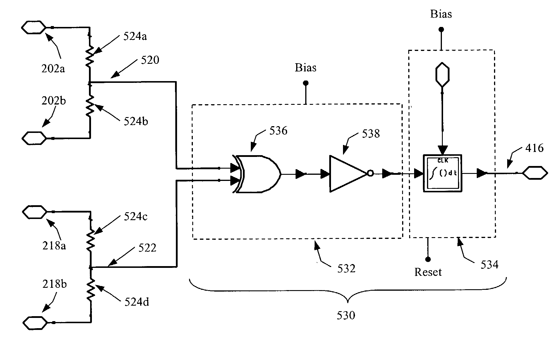
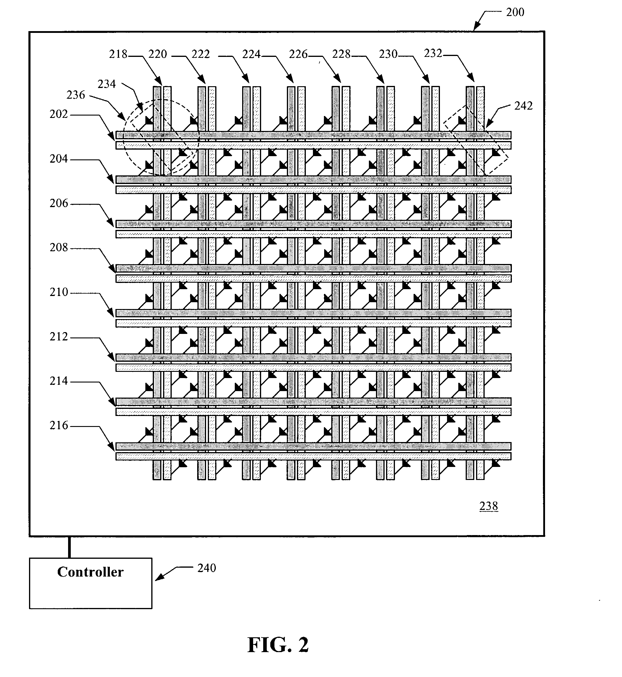
[0019]FIG. 2 depicts an embodiment of a switch matrix 200 for routing electrical signals in accordance with the present invention. The switch matrix 200 includes microstrip pairs 202–232 and switch assemblies (represented by diode pairs in FIG. 2), e.g., switch assembly 234. Switch assemblies are associated with each point where one microstrip pair crosses another, e.g., cross point 236, for electrically coupling the microstrip pairs that cross at that cross point, e.g., microstrip pairs 202, 218.

[0020]In the illustrated embodiment, the microstrip pairs 202–232 are fabricated on a semiconductor substrate 238 in a grid pattern, e.g., an 8×8 grid. A first set of the microstrip pairs, i.e., microstrip pairs 202–216, have a first orientation (horizontal) and a second set of the microstrip pairs, i.e., microstrip pairs 218–232, have a second orientation (vertical). Each microstrip pair 202–232 includes a pair of microstrips substantially parallel to one another. Preferably, the first set...


PUM


Abstract

A switch matrix including a plurality of microstrip pairs arranged to form a grid and switches to couple the microstrip pairs where they cross. Each microstrip pair includes a first microstrip and a second microstrip for passing signals. The signals on the first and second microstrips are such that the electromagnetic forces produced by each one are canceled out by the other. By canceling out the electromagnetic forces, undesirable coupling between microstrips that cross and between microstrips and the substrate are minimized, thereby allowing inexpensive substrates such as silicon to be used.

Description

FIELD OF THE INVENTION[0001]The present invention relates to the field of electronics and, more particularly, to switch matrices used in electronics to route electrical signals.BACKGROUND OF THE INVENTION[0002]Switch matrices are commonly used in the field of electronics to route electrical signals. FIG. 1 depicts a prior art switch matrix 100. The switch matrix 100 includes a plurality of overlapping microstrips 102a–102p arranged to form a grid. The microstrips are conductive lines fabricated on a semiconductor substrate 104, which is typically GaAs to minimize signal losses. At their cross points, i.e., the points where horizontal microstrips 102a–h cross vertical microstrips 102i–p, the microstrips are electrically isolated from one another. A switch (represented by the diode symbol in FIG. 1), e.g., switch 106, is present at each cross point to couple the microstrips that intersect at that cross point.[0003]Each switch can either be open (i.e., prevent an electrical connection ...

Claims


Application Information

Patent Timeline
Patent Type & Authority Patents(United States)
IPC IPC(8): H01P1/10H01P1/15H03K17/00H03K17/687H03K17/693
CPCH01P1/15H03K17/693H03K17/6874
Inventor JAIN, NITINLANTERI, JEAN-PIERREKINAYMAN, NOYAN
Owner COBHAM DEFENSE ELECTRONICS SYST CORP
Features
  • R&D
  • Intellectual Property
  • Life Sciences
  • Materials
  • Tech Scout
  • Unparalleled Data Quality
  • Higher Quality Content
  • 60% Fewer Hallucinations
Learn More