Charged-particle beam writer

a charge-particle and beam-writing technology, applied in the field of charge-particle beam-writing, can solve the problems of specimen blurring, time-consuming work, and complicated beam-writing, and achieve the effect of improving drawing accuracy

Inactive Publication Date: 2006-02-21
KK TOSHIBA
View PDF13 Cites 8 Cited by
  • Summary
  • Abstract
  • Description
  • Claims
  • Application Information

AI Technical Summary

Benefits of technology

[0010]An object of the present invention is to provide a charged-particle beam writer which causes the best dose distribution to be given for each character and the drawing dimensions to be corrected suitably and thereby improves the drawing accuracy.

Problems solved by technology

This causes a problem: the beam gets blurred on the specimen due to a space-charge effect or a so-called Boersch effect.
Changing the current density requires to adjust the electronic optical system, which needs complicated, time-consuming work.
When a character is drawn with an electron beam, dimensional errors occur due to a proximity effect or such a phenomenon as fogging.
At present, however, no consideration has been given to what dose distribution is given to which pattern on the specimen (that is, what dose is given to the scanning position).
Therefore, it is impossible to optimize the dose distribution for each character and, therefore, the drawing dimensions of each character are difficult to correct sufficiently.
Consequently, there is a possibility that the drawing accuracy will decrease.
This disadvantage may be encountered not only with an electron beam writer but also with an ion beam drawer.

Method used


Image

  • Charged-particle beam writer
  • Charged-particle beam writer
  • Charged-particle beam writer

Examples


Embodiment Construction

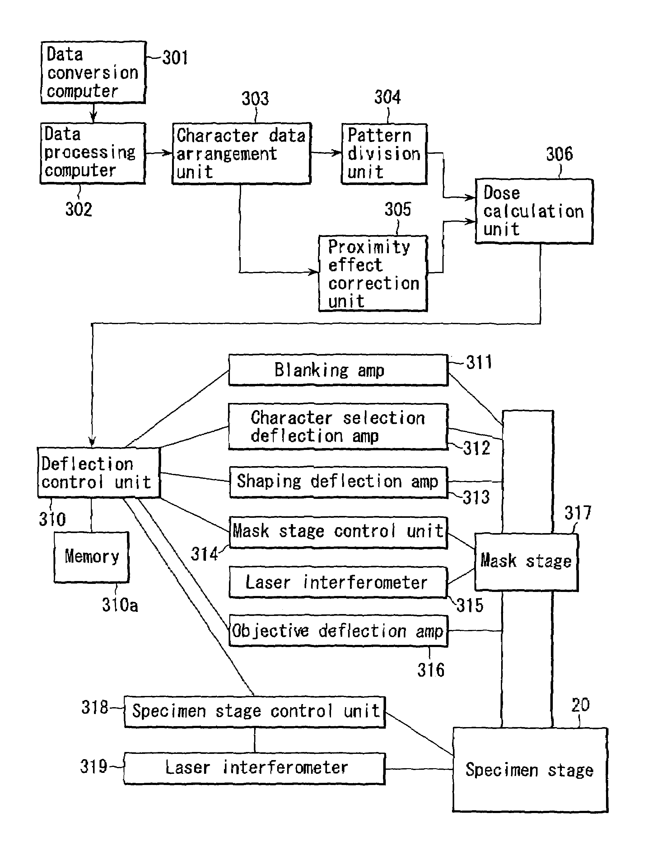
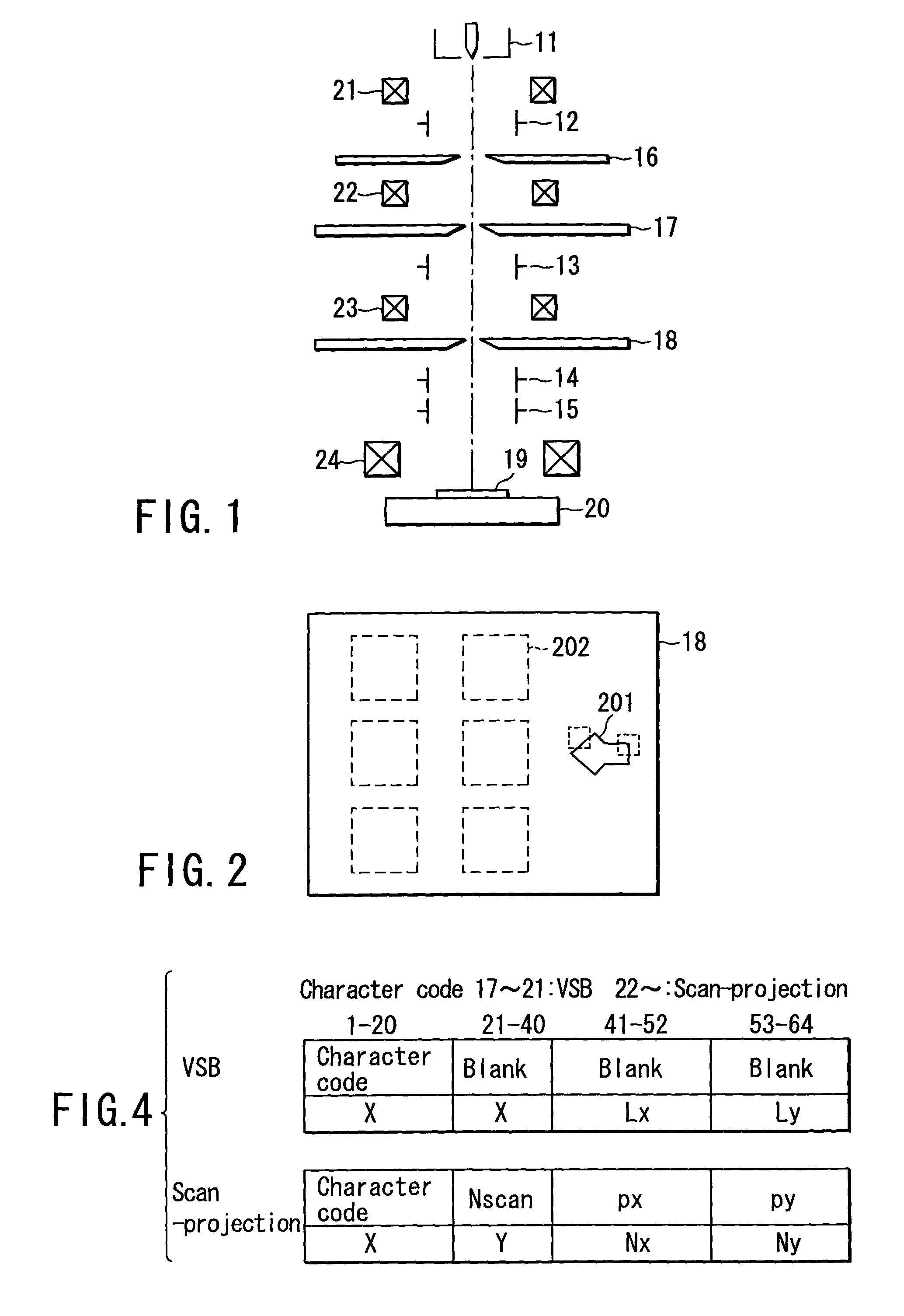
[0025]FIG. 1 shows the configuration of the optical system of an electron beam writer according to an embodiment of the present invention. In FIG. 1, numeral 11 indicates an electron gun (hereinafter, referred to as a gun 11) that produces an electron beam. Numeral 12 indicates a blanking deflector for providing on / off control of an electron beam. Numeral 13 indicates a shaping deflector for shaping a beam and selecting a character. Numeral 14 denotes a main objective deflector. Numeral 15 shows a sub-objective deflector. Numeral 16 indicates a blanking aperture mask. Numeral 17 shows a first shaping aperture mask with a rectangular aperture. Numeral 18 denotes a second shaping aperture mask with a plurality of apertures. Numeral 19 denotes a specimen. Numeral 20 shows a specimen stage. Numerals 21 to 24 indicate various types of lens systems.

[0026]An electron beam emitted from the gun 11 is projected onto the first shaping aperture mask 17 (hereinafter, referred to as the EB mask 1...


PUM

PropertyMeasurementUnit
rotation anglesaaaaaaaaaa
areaaaaaaaaaaa
radiusaaaaaaaaaa

Abstract

A charged-particle beam writer which draws a pattern on a specimen with a charged-particle beam generated from a single particle generator by both of a VSB strategy and a scan-projection strategy, the charged-particle beam writer comprising a data creating unit configured to create pattern data representing a state where a first-type figure drawn by the VSB strategy and a second-type figure drawn by the scan-projection strategy are arranged on the specimen, a computing unit configured to calculate, on the basis of the pattern data, the amount of correction for correcting the drawing dimensions of the first-type figure on the specimen and the drawing dimensions of the second-type figure on the specimen, and a control unit configured to control the dose of beam at each position on the specimen on the basis of the calculated amount of correction.

Description

CROSS-REFERENCE TO RELATED APPLICATIONS[0001]This application is based upon and claims the benefit of priority from the prior Japanese Patent Application No. 2002-285542, filed Sep. 30, 2002, the entire contents of which are incorporated herein by reference.BACKGROUND OF THE INVENTION[0002]1. Field of the Invention[0003]This invention relates to a charged-particle beam writer used to write a microscopic pattern on a semiconductor wafer. In this type of apparatus, a pattern based on, for example, CAD (Computer-Aided Design) data is formed.[0004]2. Description of the Related Art[0005]In electron beam writers used in the process of fabricating semiconductor chips, it is important to increase the throughput. For this reason, a variable-shaped beam (VSB) strategy or a character projection strategy has been applied to this type of writer in recent years (refer to, for example, Jpn. Pat. Appln. KOKAI Publication No. 2002-237445). The variable-shaped beam strategy is to produce a beam whose...

Claims


Application Information

Patent Timeline
Patent Type & Authority Patents(United States)
IPC IPC(8): H01J37/08G03F7/20H01J37/04H01J37/09H01J37/147H01J37/305H01J37/317H01L21/027
CPCB82Y10/00B82Y40/00H01J37/3174H01J37/3175H01J2237/31776H01J2237/31762H01J2237/31764H01J2237/31769
Inventor OGASAWARA, MUNEHIRO
Owner KK TOSHIBA
Why Eureka
Try Eureka