Image recording medium having suppression layer for suppressing interfacial crystallization
a technology of interfacial crystallization and suppression layer, which is applied in the field of image recording medium, can solve the problems of deterioration of sensitivity and remaining of ghost images, and achieve the effect of suppressing interfacial crystallization and forming a layer
- Summary
- Abstract
- Description
- Claims
- Application Information
AI Technical Summary
Benefits of technology
Problems solved by technology
Method used
Image
Examples
first embodiment
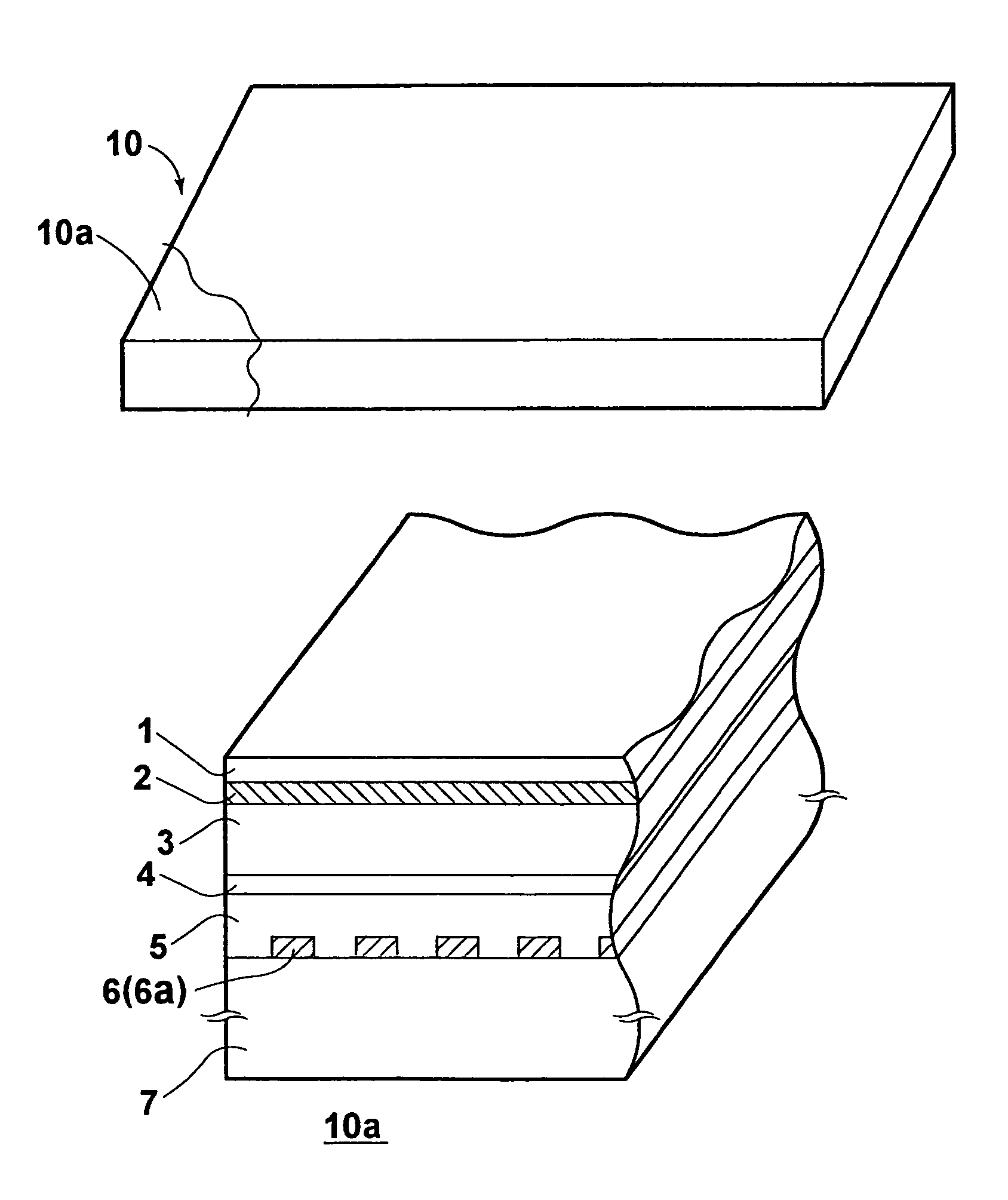
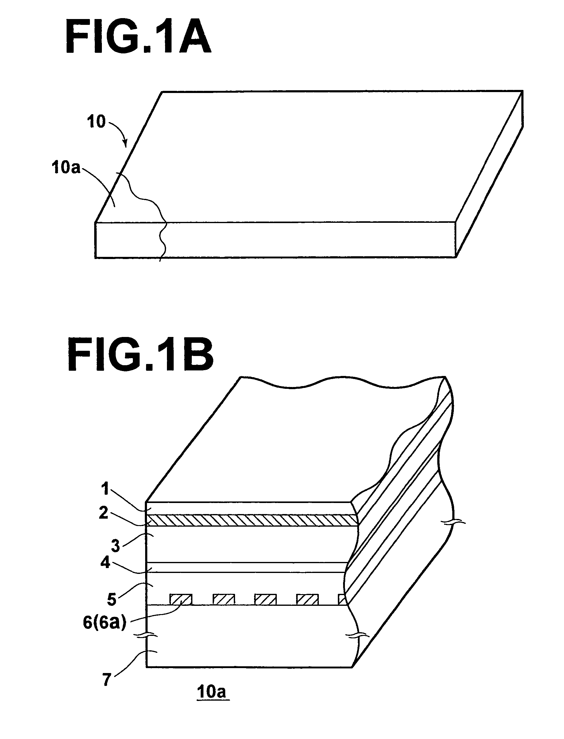
[0029]FIG. 1A is a perspective view of a radiographic-image recording medium as a first embodiment of the image recording medium according to the present invention, and FIG. 1B is a magnified perspective view of a cutaway portion 10a of the radiographic-image recording medium 10 of FIG. 1A, where a cross section of the cutaway portion 10a is illustrated.
[0030]The radiographic-image recording medium 10 illustrated in FIGS. 1A and 1B comprises a first electrode layer 1, a suppression layer 2, a recording-side photoconductive layer 3, a charge storage region 4, a reading-side photoconductive layer 5, a second electrode layer 6, and a substrate 7 are arranged in this order.
[0031]The first electrode layer 1 is transparent to radiation for recording. The suppression layer 2 is arranged between the first electrode layer 1 and the recording-side photoconductive layer 3, and prevents interfacial crystallization in the recording-side photoconductive layer 3. The recording-side photoconductive...
second embodiment
[0046]FIG. 3A is a perspective view of a radiographic-image recording medium of an indirect-conversion type according to the second embodiment of the image recording medium according to the present invention, and FIG. 3B is a magnified perspective view of a cutaway portion 20a of the radiographic-image recording medium 20 of FIG. 3A, where a cross section of the cutaway portion 20a is illustrated.
[0047]The radiographic-image recording medium 20 illustrated in FIGS. 3A and 3B comprises a fluorescent layer 21, a first electrode layer 31, a suppression layer 32, a recording-side photoconductive layer 33, a charge storage region 34, a reading-side photoconductive layer 35, a second electrode layer 36, and a substrate 37 are arranged in this order.
[0048]The fluorescent layer 21 contains a fluorescent material which converts radiation (for recording) into visible light. The first electrode layer 31 is transparent to the visible light emitted from the fluorescent layer 21. The suppression ...
PUM
| Property | Measurement | Unit |
|---|---|---|
| thickness | aaaaa | aaaaa |
| thicknesses | aaaaa | aaaaa |
| thickness | aaaaa | aaaaa |
Abstract
Description
Claims
Application Information


