Semiconductor memory device with a decoupling capacitor

a memory device and capacitor technology, applied in the direction of information storage, static storage, digital storage, etc., can solve the problems of large current consumption, power noise, and large current consumption, and achieve the effect of reducing power noise and improving operating speed

Inactive Publication Date: 2006-02-21
SAMSUNG ELECTRONICS CO LTD
View PDF6 Cites 6 Cited by
  • Summary
  • Abstract
  • Description
  • Claims
  • Application Information

AI Technical Summary

Benefits of technology

[0007]It is another object of the invention to provide a semiconductor memory device capable of reducing power noise.
[0008]It is yet another object of the invention to provide a semiconductor memory device capable of improving operating speed.

Problems solved by technology

Read and write operations consume larger current amounts.
This large current consumption decreases a power supply voltage and increases a ground voltage creating a power noise when performing a read or write operation.
Decreasing the operating speed may further drain the power supply voltage.

Method used


Image

  • Semiconductor memory device with a decoupling capacitor
  • Semiconductor memory device with a decoupling capacitor
  • Semiconductor memory device with a decoupling capacitor

Examples


first embodiment

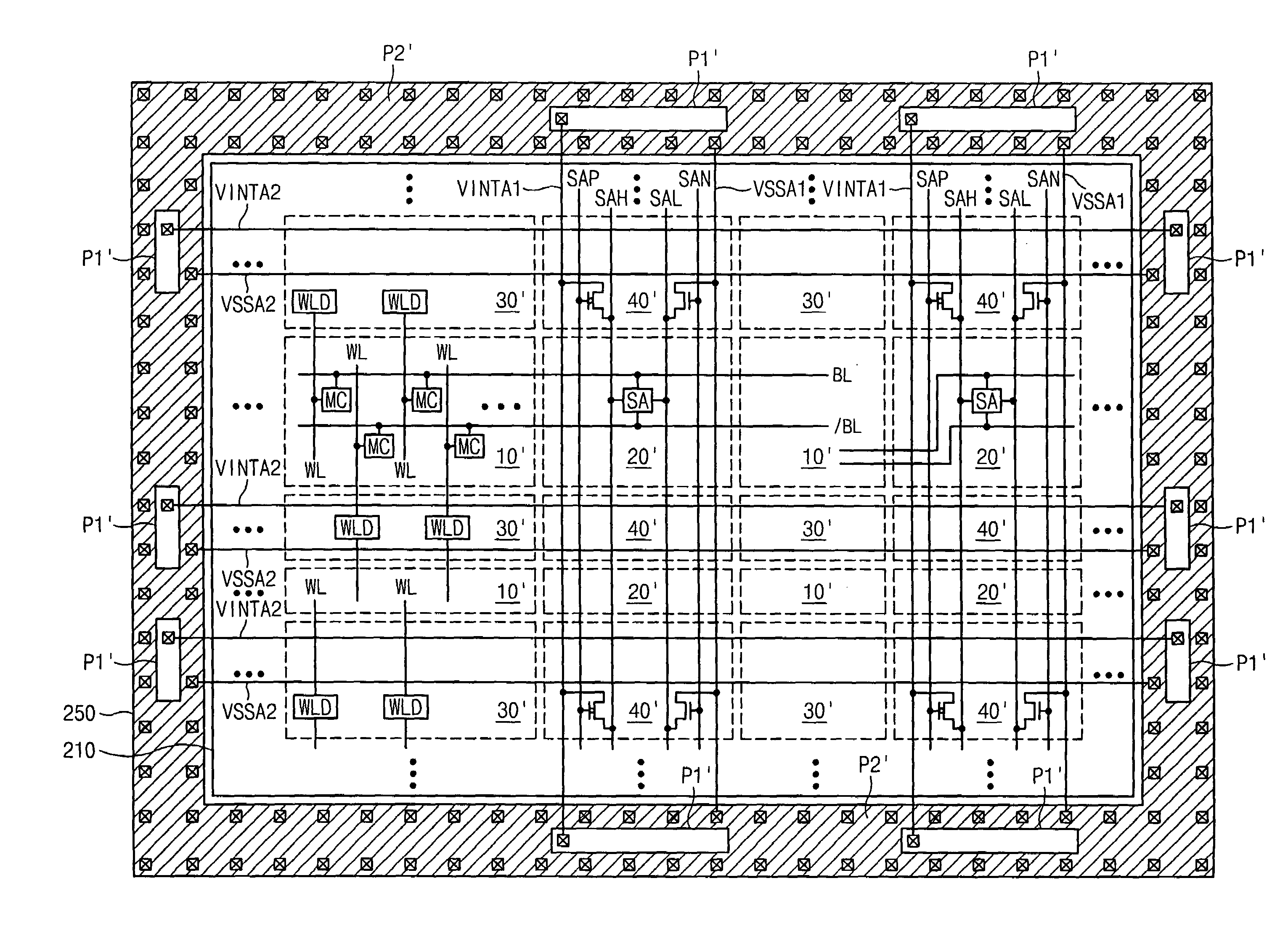
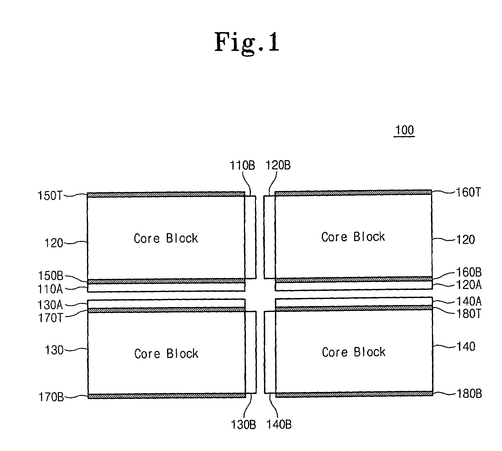
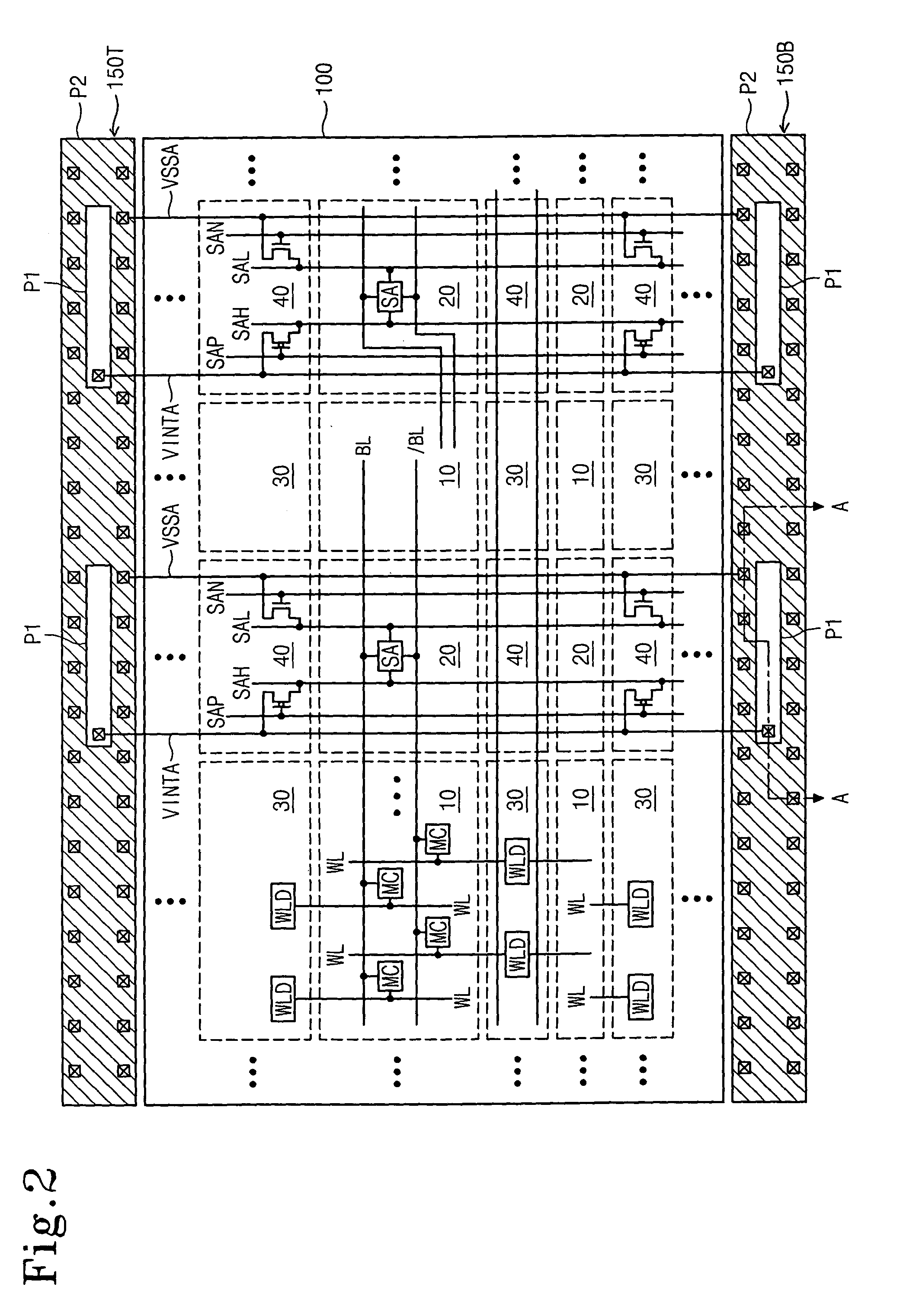
[0021]FIG. 1 is a block diagram of a semiconductor memory device according to the present invention. Referring to FIG. 1, a semiconductor memory device 100 of the present invention comprises a plurality of, core blocks, e.g. blocks 110, 120, 130, and 140, arranged in a matrix shape. A row selector block is disposed at one side and a column selector block is disposed at the other side of a corresponding core block. For example, a row selector block 110A is disposed at a bottom side of a core block 110 and a column selector block 110B is disposed at a right side of the block 110. A row selector block 120A is disposed at a bottom side of a core block 120 and a column selector block 120B is disposed at a left side thereof. A row selector block 130A is disposed at a top side of a core block 130 and a column selector block 130B is disposed at a right side thereof. A row selector block 140A is disposed at a top side of a core block 140 and a column selector block 140B is disposed at a left...

third embodiment

[0043]FIG. 6 shows a block diagram of a semiconductor memory device according to the present invention.

[0044]Referring to FIG. 6, a semiconductor memory device 300 of the present invention comprises a plurality of core blocks, e.g. core blocks 310, 320, 330 and 340, arranged in a matrix shape. A row selector block is disposed at one side of a core block and a column selector block is disposed at another side thereof. For example, a row selector block 310A is disposed at a bottom side of a core block 310 and a column selector block 310B is disposed at a right side thereof. A row selector block 320A is disposed at a bottom side of a core block 320, and a column selector block 320B is disposed at a left side thereof. A row selector block 330A is disposed at a top side of a core block 330 and a column selector block 330B is disposed at a right side thereof. A row selector block 340A is disposed at a top side of a core block 340 and a column selector block 340B is disposed at a left side...


PUM


Abstract

A semiconductor memory device includes a core block having sub-arrays and sense amplifier regions. First and second charge storing regions are disposed at sides of the core block. First and second decoupling capacitors are formed at the first and second charge storing regions, respectively. A plurality of first voltage supply lines are disposed to supply a power supply voltage to the sense amplifier regions and are connected to one electrode of each of the first and second decoupling capacitors. A plurality of second voltage supply lines are disposed to supply a ground voltage to the sense amplifier regions and are connected to the other electrode of each of the first and second decoupling capacitors.

Description

[0001]This application claims priority from Korean Patent Application No. 2003-04196, filed on Jan. 22, 2003, the contents of which are incorporated by reference in their entirety.FIELD OF THE INVENTION[0002]The present invention relates to a semiconductor memory device and, more particularly, to a random access memory device with a decoupling capacitor.BACKGROUND OF THE INVENTION[0003]A semiconductor memory device includes a memory cell array for storing data information. Data, e.g. 0 or 1, is written in or read out from each memory cell of the array. Read and write operations can be carried out by a read means and a write means, respectively, or by one read / write means depending on a semiconductor memory device. In the case of DRAM devices, for example, read and write operations are carried out through a well-known sense amplifier. In the case of SRAM devices, a read operation is carried out by a sense amplifier and a write operation is carried out by a write driver.[0004]An examp...

Claims


Application Information

Patent Timeline
Patent Type & Authority Patents(United States)
IPC IPC(8): G11C8/00G11C7/00G11C5/06
CPCG11C5/063G11C7/00
Inventor HWANG, HYONG-RYOLSEO, YOUNG-HUNSIM, JAE-YOON
Owner SAMSUNG ELECTRONICS CO LTD
Why Eureka
Try Eureka