Memory control chip, control method and control circuit
- Summary
- Abstract
- Description
- Claims
- Application Information
AI Technical Summary
Benefits of technology
Problems solved by technology
Method used
Image

Examples
Embodiment Construction
[0022]Reference will now be made in detail to the present preferred embodiments of the invention, examples of which are illustrated in the accompanying drawings. Wherever possible, the same reference numbers are used in the drawings and the description to refer to the same or like parts.
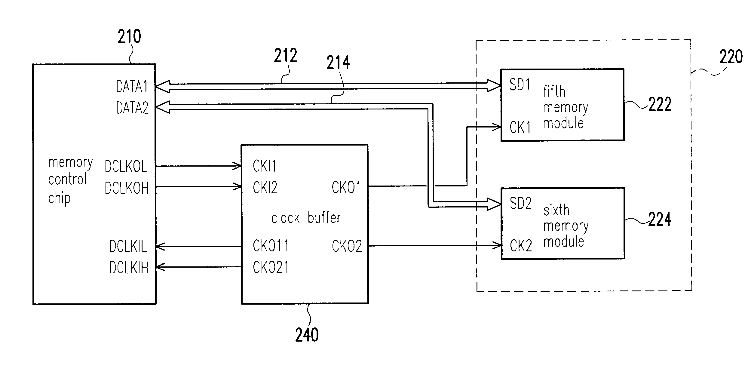
[0023]FIG. 3 is a block diagram of a memory control circuit with a 128-bit data bus architecture according to one preferred embodiment of this invention. As shown in FIG. 3, the circuit includes a memory control chip 210, a clock buffer 240, a fifth memory module 222 and a sixth memory module 224. Both the fifth memory module 222 and the sixth memory module 224 belong to a memory bank 220 but plugged into separate memory module slots (not shown).
[0024]The data signal leads (DATA1 and DATA2) of the memory control chip 210 are 128-bit wide. The data signal leads (SD1 and SD2) of the fifth memory module 222 and the sixth memory module 224 are 128-bit wide. So, the memory control chip 210 can use a 128-b...
PUM
 Abstract
Description
Claims
Application Information
 - R&D
- Intellectual Property
- Life Sciences
- Materials
- Tech Scout
- Unparalleled Data Quality
- Higher Quality Content
- 60% Fewer Hallucinations
Browse by: Latest US Patents, China's latest patents, Technical Efficacy Thesaurus, Application Domain, Technology Topic, Popular Technical Reports.
© 2025 PatSnap. All rights reserved.Legal|Privacy policy|Modern Slavery Act Transparency Statement|Sitemap|About US| Contact US: help@patsnap.com