
Method of manufacturing inorganic nanotube

a manufacturing method and nanotube technology, applied in the direction of polycrystalline material growth, crystal growth process, chemically reactive gas, etc., can solve the problem that the method of manufacturing inorganic nanotubes in a systematic array using vapor deposition is virtually unknown, and is suitable for manufacturing nano-scale devices

Inactive Publication Date: 2006-02-28
SAMSUNG ELECTRONICS CO LTD
View PDF7 Cites 389 Cited by
  • Summary
  • Abstract
  • Description
  • Claims
  • Application Information

AI Technical Summary

Benefits of technology

This approach allows for the accurate and controlled manufacturing of inorganic nanotubes with precise thickness and structure, compatible with semiconductor technology, enabling the production of inorganic nanotubes in various shapes and arrays without requiring separate etching processes.

Problems solved by technology

However, a method of manufacturing inorganic nanotubes in a systematic array using vapor deposition suitable for manufacturing of nano-scale devices is virtually unknown.

Method used


Image

  • Method of manufacturing inorganic nanotube
  • Method of manufacturing inorganic nanotube
  • Method of manufacturing inorganic nanotube

Examples


Embodiment Construction

[0023]Korean Patent Application No. 2002-34293, filed on Jun. 19, 2002, and entitled: “Method of Manufacturing Inorganic Tubes,” is incorporated by reference herein in its entirety.

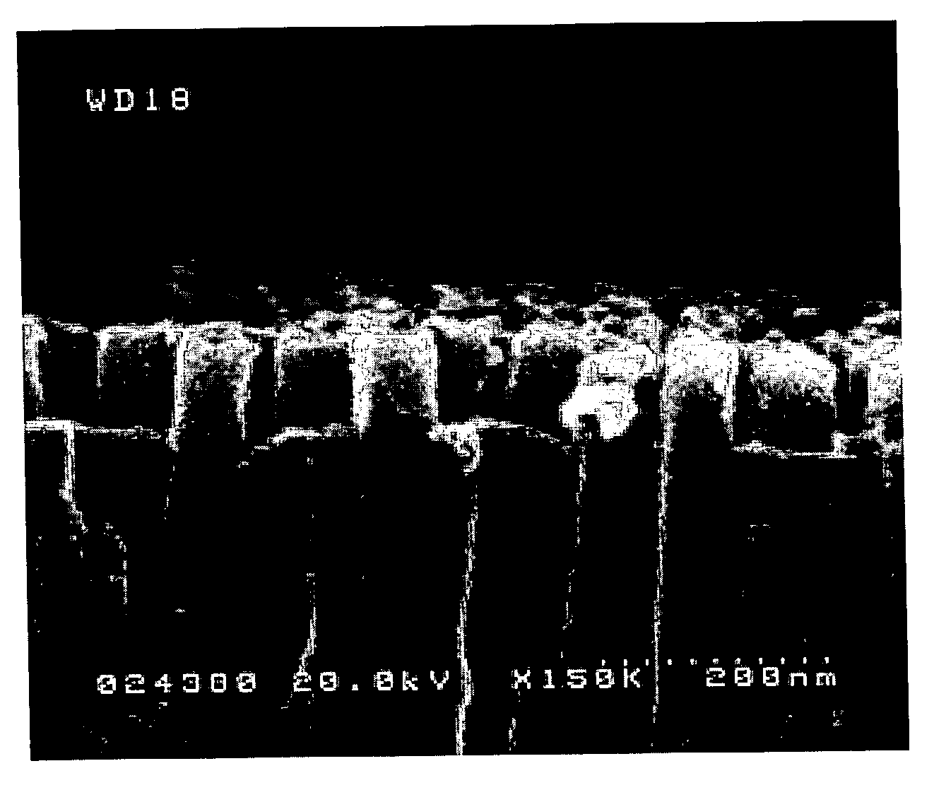
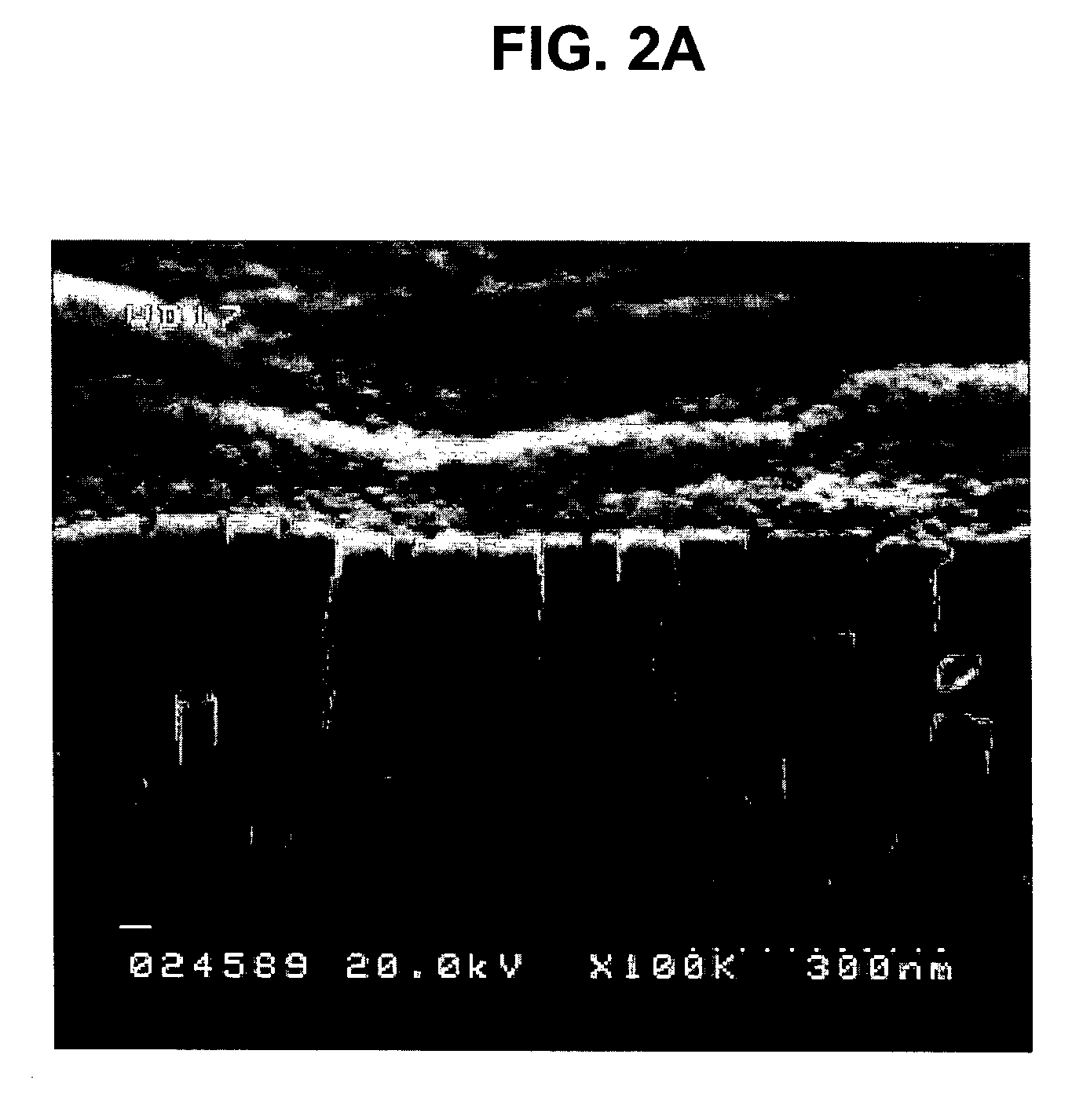
[0024]According to an embodiment of the present invention, a method of manufacturing an inorganic nanotube or an array of inorganic nanotubes uses a carbon nanotube (CNT) or an array of CNTs is used as a template. In other words, a CNT or an array of CNTs is coated with an inorganic thin film for an inorganic nanotube using atomic layer deposition (ALD). Deposition behavior of the inorganic thin film formed using ALD is different on the inner wall and on the outer wall of the CNT. The inorganic thin film formed on the inner wall of the CNT has a sparse micro structure. Accordingly, when the inorganic thin film is processed in an activated oxidation atmosphere such as an oxygen, ozone, or plasma atmosphere, the CNT combusts, and a new second inorganic nanotube or an array of second inorganic nanotubes is f...


PUM

PropertyMeasurementUnit
temperatureaaaaaaaaaa
timeaaaaaaaaaa

Abstract

A method of manufacturing an inorganic nanotube using a carbon nanotube (CNT) as a template, includes preparing a template on which a CNT or a CNT array is formed, forming an inorganic thin film on the CNT by depositing an inorganic material on the template using atomic layer deposition (ALD), and removing the CNT to obtain an inorganic nanotube or an inorganic nanotube array, respectively.

Description

BACKGROUND OF THE INVENTION[0001]1. Field of the Invention[0002]The present invention relates to a method of manufacturing an inorganic nanotube or an array of inorganic nanotubes and, more particularly, to a method of manufacturing an inorganic nanotube using a carbon nanotube as a template.[0003]2. Description of the Related Art[0004]With recent development of integrated and compact optical and electronic devices, nano-structured materials and manufacturing methods thereof have been actively researched and developed. Various methods of manufacturing nano-scale rods, wires, tubes, and particles using various materials have been widely studied. However, a method of manufacturing inorganic nanotubes in a systematic array using vapor deposition suitable for manufacturing of nano-scale devices is virtually unknown.SUMMARY OF THE INVENTION[0005]The present invention provides a method of manufacturing various types of inorganic nanotubes, especially a method of manufacturing an inorganic...

Claims


Application Information

Patent Timeline
Patent Type & Authority Patents(United States)
IPC IPC(8): H01L21/31B82B3/00C01B31/02C01G55/00C23C14/14C23C16/01C23C16/40C23C16/44C30B25/00
CPCB82Y30/00B82Y40/00C01B31/0233C01G55/00C30B25/00C30B29/605C01B2202/08C01P2004/03Y10S977/893C01P2004/13C01P2004/64C01P2004/04C01B32/162B82B3/00C23C16/01
Inventor MIN, YO-SEPBAE, EUN-JUCHOI, WON-BONGCHO, YOUNG-JINLEE, JUNG-HYUN
Owner SAMSUNG ELECTRONICS CO LTD
Learn More