Metal-oxide-semiconductor device having improved performance and reliability

a technology of metal-oxide-semiconductor and mos, which is applied in the direction of mos devices, basic electric elements, electrical apparatus, etc., can solve the problems of achieve the effects of reducing undesirable effects, improving performance and reliability, and not significantly increasing the cost of manufacturing ic devices

Inactive Publication Date: 2006-02-28
BELL SEMICON LLC
View PDF6 Cites 28 Cited by
  • Summary
  • Abstract
  • Description
  • Claims
  • Application Information

AI Technical Summary

Benefits of technology

[0007]The present invention provides techniques for reducing undesirable effects including HCI, current crowding, and / or high electric field distribution in an MOS device, thereby improving performance and reliability without undesirably affecting high-frequency performance of the device. Moreover, the techniques of the present invention can be used to fabricate an integrated circuit (IC) device, for example, an LDMOS device, using conventional CMOS compatible process technology. Consequently, the cost of manufacturing the IC device is not significantly increased.
[0009]The at least one trench is preferably configured such that as a voltage at the second source / drain region increases, a depletion region spreads outward from the trench so as to substantially fill a region proximate the trench. The MOS device provides reduced HCI effects, reduced current crowding and / or a reduced peak electric field near the gate, particularly in an area proximate the upper surface of the semiconductor layer, without substantially degrading high-frequency performance. Furthermore, the MOS device is substantially compatible with a CMOS process technology.

Problems solved by technology

Consequently, the cost of manufacturing the IC device is not significantly increased.

Method used


Image

  • Metal-oxide-semiconductor device having improved performance and reliability
  • Metal-oxide-semiconductor device having improved performance and reliability
  • Metal-oxide-semiconductor device having improved performance and reliability

Examples


Embodiment Construction

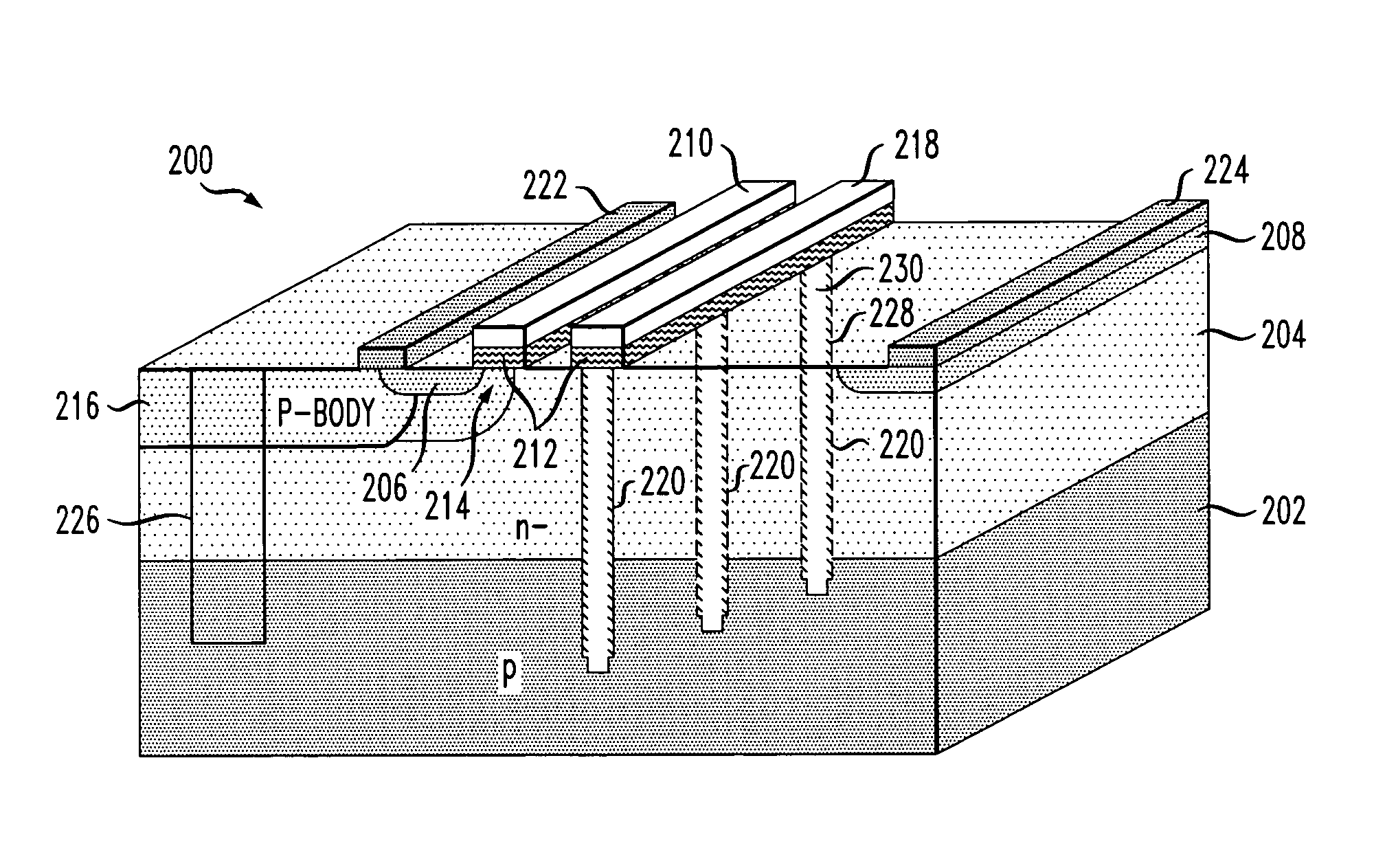
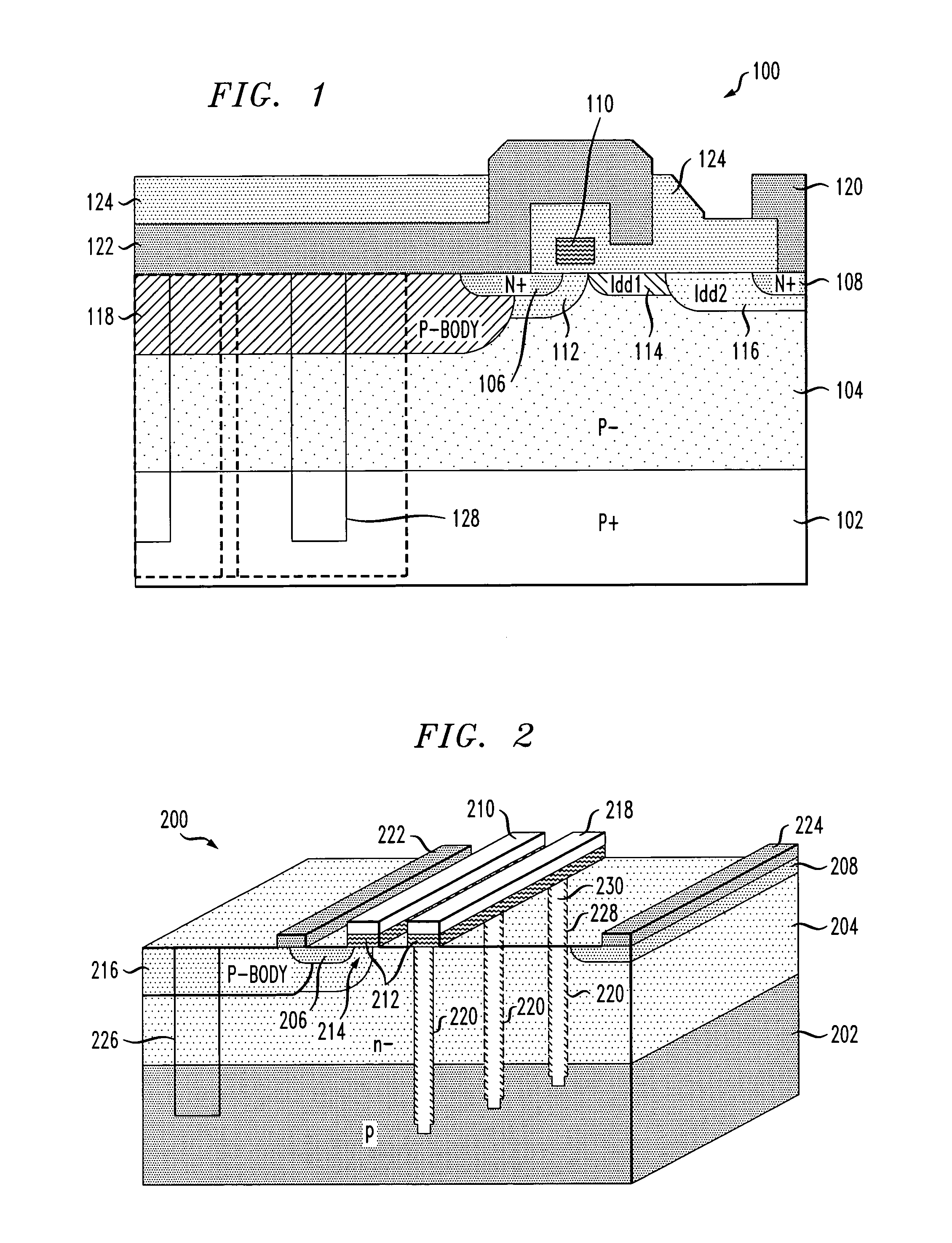
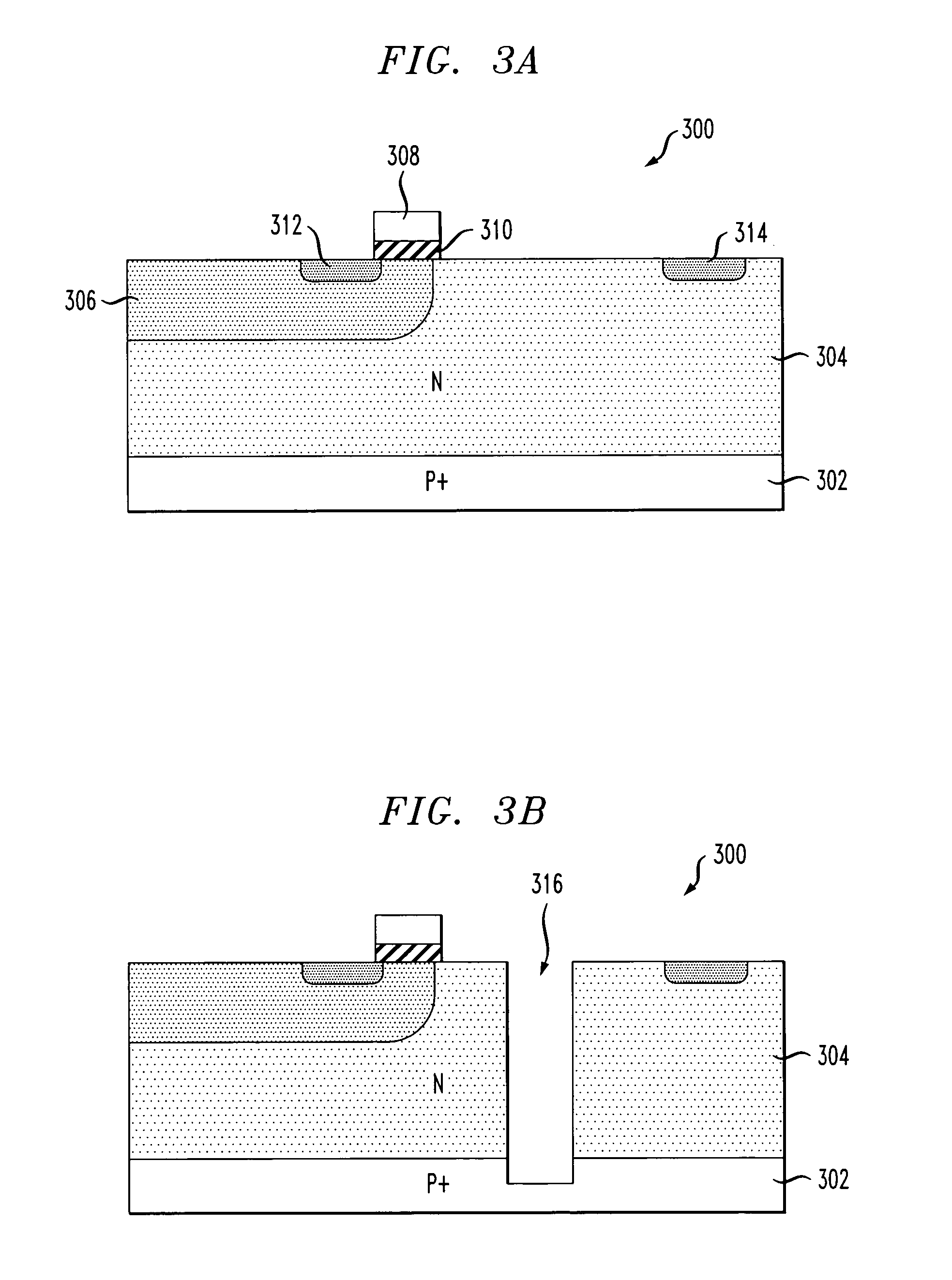
[0014]The present invention will be described herein in the context of an illustrative CMOS integrated circuit fabrication technology suitable for forming discrete RF LDMOS transistors, as well as other devices and / or circuits. It should be appreciated, however, that the present invention is not limited to the fabrication of this or any particular device or circuit. Rather, the invention is more generally applicable to any MOS device in which it is desirable to alleviate effects including HCI, current crowding and / or high electric field distribution, thereby improving the performance and reliability of the device without significantly affecting high-frequency performance in the device.

[0015]Although implementations of the present invention are described herein with specific reference to an LDMOS device, it is to be appreciated that the techniques of the present invention are similarly applicable to other devices, such as, but not limited to, a vertical diffused MOS (DMOS) device, an...


PUM


Abstract

An MOS device includes a semiconductor layer comprising a substrate of a first conductivity type and a second layer of a second conductivity type formed on at least a portion of the substrate. First and second source / drain regions of the second conductivity type are formed in the second layer proximate an upper surface of the second layer, the second layer being spaced laterally from the first source / drain region. A gate is formed above the second layer proximate the upper surface of the second layer and at least partially between the first and second source / drain regions. The MOS device further includes at least one electrically conductive trench formed in the second layer between the gate and the second source / drain region, the trench being formed proximate the upper surface of the semiconductor layer and extending substantially vertically through the second layer to the substrate. The MOS device exhibits reduced HCI effects and / or improved high-frequency performance.

Description

FIELD OF THE INVENTION[0001]The present invention relates generally to semiconductor devices, and more particularly relates to techniques for forming an MOS device having improved reliability without significantly-impacting high-frequency performance.BACKGROUND OF THE INVENTION[0002]Power MOS devices, including laterally diffused metal-oxide-semiconductor (LDMOS) devices, are employed in a variety of applications, such as, for example, power amplifiers in wireless communications systems. In a conventional LDMOS device, hot-carrier injection (HCI) effects, current crowding in a lightly-doped drain (LDD) region and / or electric field distribution are some of the phenomena which are known to undesirably affect the performance and reliability of the device.[0003]HCI in an MOS device generally results from heating and subsequent injection of carriers into the gate oxide of the device, which results in a localized and nonuniform buildup of interface states and oxide charges near and undern...

Claims


Application Information

Patent Timeline
Patent Type & Authority Patents(United States)
IPC IPC(8): H01L29/94H01L29/78H01L29/06H01L29/10H01L29/40H01L29/417H01L29/76
CPCH01L29/0634H01L29/1083H01L29/402H01L29/407H01L29/4175H01L29/7816H01L29/7835H01L21/02293H01L29/41725H01L29/7848H01L29/94
Inventor SHIBIB, MUHAMMED AYMANXU, SHUMING
Owner BELL SEMICON LLC
Why Eureka
Try Eureka