Method of testing electronic wafers having lead-free solder contacts

a technology of electronic wafers and solder contacts, applied in electrical testing, measurement devices, instruments, etc., can solve the problems of affecting the quality of electronic wafers, and requiring complex fabrication techniques, etc., to reduce the variability of contact resistance, eliminate the sliding movement of the probe tip, and reduce the contact resistance

Active Publication Date: 2006-02-28
BELL SEMICON LLC
View PDF1 Cites 6 Cited by
  • Summary
  • Abstract
  • Description
  • Claims
  • Application Information

AI Technical Summary

Benefits of technology

[0009]In accordance with one aspect of our invention, we have devised a cantilever probe method of parametrically testing wafers that extends the probe tip cleaning interval, maintains relatively low contact resistance, and reduces contact resistance variability. In one embodiment of our invention, a method of testing electronic circuits, formed in a wafer having lead-free terminals, comprises the steps of: exposing the terminals to a plasma containing oxygen; providing a test apparatus having probes for contacting the terminals; and bringing the probe tips into contact with selected ones of the terminals, so as to perform electrical tests on the wafer; and, during the contacting step, exposing the probe tips to the flow of a non-oxidizing gas (e.g., nitrogen, argon). In a preferred embodiment, the terminals are Sn-based solder bumps. In another preferred embodiment, the probe tip comprises BeCu. In yet another preferred embodiment, each probe has a cantilevered probe arm and a probe tip extending from the arm at an acute angle α, the angle α being designed to essentially eliminate sliding movement of the probe tip when in contact with a terminal. Illustratively, the angle α is approximately 87°–90°.

Problems solved by technology

When the semiconductor devices are sensitive to contact resistance, as many are, such parametric testing apparatus has a persistent problem—the probe tips become contaminated and / or worn, necessitating frequent cleaning and / or replacement.
Although the vertical probe card design can provide reliable contact resistance and an acceptable number of probe tip cleanings, it is an expensive solution; that is, complex fabrication techniques are required to manufacture the head 10.2 and the router-substrate 10.4.
On the other hand, cantilever probe cards are less expensive initially (e.g., $3,000 to $4,000), but require frequent probe tip cleanings, which reduces probe tip life.
In addition, incorrectly setting the probe cleaning interval can adversely affect yield.
Yield can be adversely affected by changes in device parameters that are influenced by increased contact resistance; e.g., manufacturing variations in the composition of the terminals can potentially impact the cleaning frequency by the way material accumulates on the probes and the corresponding increase of contact resistance prior to the predicted cleaning interval.

Method used


Image

  • Method of testing electronic wafers having lead-free solder contacts
  • Method of testing electronic wafers having lead-free solder contacts
  • Method of testing electronic wafers having lead-free solder contacts

Examples


example

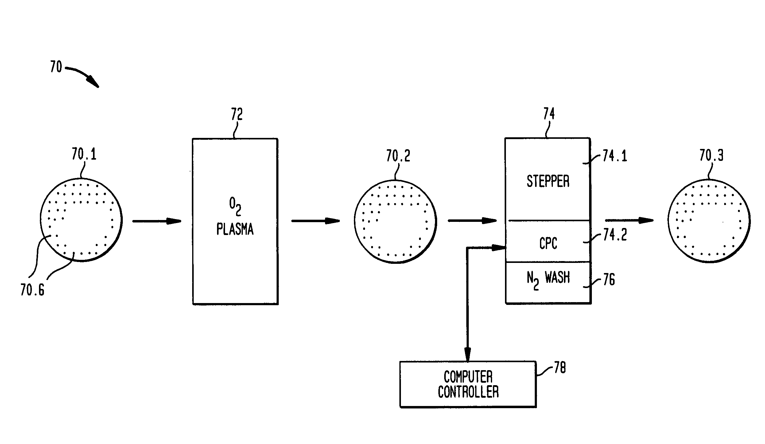
[0026]This example describes a method of testing electronic eight-inch wafers having lead-free, solder bumps, in accordance with one embodiment of our invention. Each wafer contained about 2500 integrated circuits (dies) that performed pre-amplifier functions. Various materials, dimensions and operating conditions are provided by way of illustration only and, unless otherwise expressly stated, are not intended to limit the scope of the invention.

[0027]More specifically, the electronic wafers had metal solder bumps comprising a 95% Sn-3.5% Ag-1.5% Cu alloy. The wafers were maintained at about 25° C. and were oxidized in a commercially available plasma reactor under the following conditions:

[0028]

RF power475 WattsVacuum138 mTorrO2 flow rate80 cc / mm @ 5–10 psiPlasma modeDownstreamTime≧1 min

[0029]To demonstrate the effect of the plasma process we turn to FIGS. 6–7, which are Auger depth profiles of the wafer before (FIG. 6) and after (FIG. 7) it had been subjected to the oxygen plasma. ...


PUM


Abstract

A cantilever probe method of parametrically testing wafers extends the probe tip cleaning interval, maintains relatively low contact resistance, and reduces contact resistance variability. In one embodiment of our invention, a method of testing electronic circuits formed in a wafer having lead-free terminals, comprises the steps of exposing the terminals to a plasma containing oxygen; providing a test apparatus having cantilevered probes for contacting the terminals; each probe having a cantilevered probe arm and a BeCu probe tip extending from the arm at an acute angle α; the angle α being designed to essentially eliminate sliding movement of the probe tip when in contact with a terminal; and bringing the probe tips into contact with selected ones of the terminals, so as to perform electrical tests on the wafer; and, during the contacting step, exposing the probe tips to a flow of a non-oxidizing gas (e.g, nitrogen, argon). In a preferred embodiment, the terminals are Sn-based solder bumps. In another preferred embodiment the angle α is approximately 87°–90°.

Description

BACKGROUND OF THE INVENTION[0001]1. Field of the Invention[0002]This invention relates to a method of testing electronic circuits and / or semiconductor devices in wafer form and, more particularly, to a method of testing such circuits / devices in wafers having lead-free solder bump contacts.[0003]2. Discussion of the Related Art[0004]In the industry of semiconductor devices (e.g., integrated circuits and discrete devices) it is common to parametrically test the circuits / devices while they are still an integral part of a semiconductor wafer; that is, before the wafer has been diced into individual circuits or chips. To do so, the test apparatus typically includes a probe card, which has a nest of electrical probes that enable the apparatus to make electrical contact with a subset of terminals (e.g., bond pads, solder bumps) on the wafer. Once testing of a subset of terminals is complete, the wafer is moved laterally relative to the probe card (e.g., via a well known stepper machine) so...

Claims


Application Information

Patent Timeline
Patent Type & Authority Patents(United States)
IPC IPC(8): G01R31/26
CPCG01R31/2831
Inventor BUSS, BRIAN LEEICKES, JR., ROBERT DALERADEMACHER, WAYNE ALAN
Owner BELL SEMICON LLC
Why Eureka
Try Eureka