Concurrent measurement and cleaning of thin films on silicon-on-insulator (SOI)

a technology of silicon-on-insulator and thin film, applied in the field of measurement systems, to achieve the effect of accurate swe measurements

Inactive Publication Date: 2006-02-28
KLA TENCOR TECH CORP
View PDF27 Cites 23 Cited by
  • Summary
  • Abstract
  • Description
  • Claims
  • Application Information

AI Technical Summary

Benefits of technology

[0015]The invention provides a system and method for accurate SWE measurements on multi-layer substrates such as SOI. By using a measurement beam having an absorption distance that is less than the thickness of the superficial layer of the multi-layer substrate, spurious reflections at layers beneath the superficial layer are eliminated.
[0016]According to an embodiment of the invention, a SWE system configured to generate a measurement beam having an absorption distance less than the superficial layer thickness of a multi-layer substrate can also include a cleaning beam generator to perform localized cleaning before and during SWE operations to improve measurement accuracy. By performing concurrent cleaning and measurement operations, SWE accuracy can be enhanced without significantly affecting measurement throughput.

Problems solved by technology

For example, each pulse of a laser cleaning beam could cause localized heating of the test sample that could in turn affect measurements taken at this elevated temperature.

Method used


Image

  • Concurrent measurement and cleaning of thin films on silicon-on-insulator (SOI)
  • Concurrent measurement and cleaning of thin films on silicon-on-insulator (SOI)
  • Concurrent measurement and cleaning of thin films on silicon-on-insulator (SOI)

Examples


Embodiment Construction

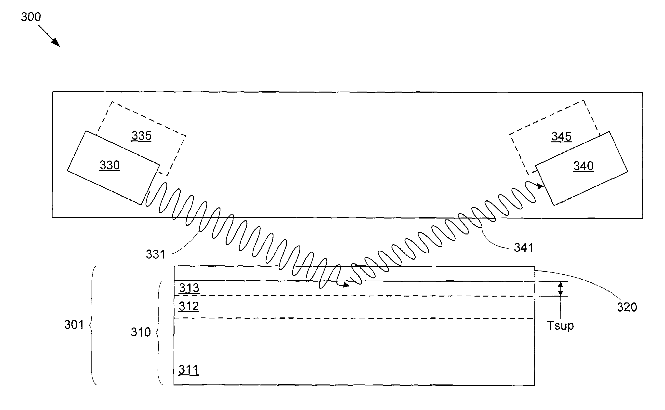
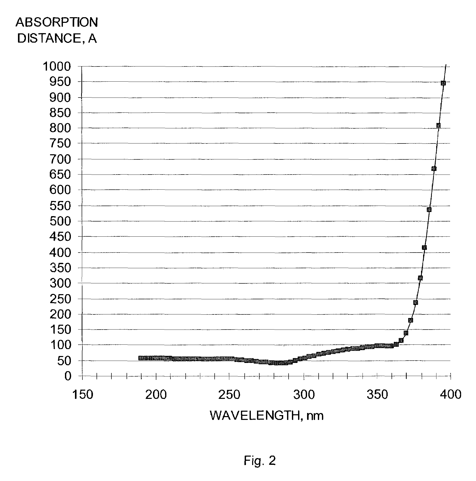
[0028]By matching the wavelength of a measurement beam in a SWE system with the superficial silicon layer thickness in an SOI substrate, the invention enables the use of SWE to measure thin film thickness on SOI substrates. By selecting the measurement beam wavelength such that the absorption distance of the measurement beam is less than the thickness of the superficial silicon layer of the SOI substrate, spurious reflections at the interface between the superficial silicon layer and buried insulator layer can be eliminated.

[0029]Absorption distance in a particular material (such as silicon) is defined by the equation:

D=λ / (4πk)  (1)

where D is the absorption distance, λ is the wavelength of the measurement beam in the material, and k is the extinction coefficient for the material. Values for the extinction coefficient k of various materials are readily available from published literature. Note that in a material such as doped silicon, the value of extinction coefficient k will be aff...


PUM


Abstract

A system for performing single wavelength ellipsometry (SWE) on a thin film on a multi-layer substrate such as silicon-on-insulator (SOI) applies a measurement beam having an absorption distance less than the thickness of the superficial layer of the multi-layer substrate. For example, for an SOI substrate, the measurement beam is selected to have a wavelength that results in an absorption distance that is less than the superficial silicon layer thickness. The system can include a cleaning laser to provide concurrent cleaning to enhance measurement accuracy without negatively impacting throughput. The measurement beam source can be configured to provide a measurement beam at one wavelength and a cleaning beam at a longer wavelength, so that the absorption depth of the measurement beam is less than the superficial layer thickness while the absorption depth of the cleaning beam is greater than the superficial layer thickness.

Description

FIELD OF THE INVENTION[0001]This invention relates generally to measurement systems, and more particularly to a system and method for performing metrology on silicon-on-insulator structures.BACKGROUND OF THE INVENTION[0002]As the dimensions of semiconductor devices continue to shrink, accurate and efficient characterization of the components forming those devices becomes more critical. Typically, the manufacturing process for modern semiconductor devices includes the formation of a number of layers or “thin films” on a silicon wafer. The thin films can include oxide, nitride, and / or metal layers, among others. To ensure proper performance of the finished semiconductor devices, the thickness and composition of each thin film formed during the manufacturing process must be tightly controlled.[0003]Single wavelength ellipsometry (SWE) is a technique for measuring thin film thickness by directing a single wavelength polarized beam at a thin film, and then measuring the change in polariz...

Claims


Application Information

Patent Timeline
Patent Type & Authority Patents(United States)
IPC IPC(8): G01J4/00G01B11/06
CPCG01B11/06G01J4/00G01B11/065
Inventor KRISHNAN, SHANKAR
Owner KLA TENCOR TECH CORP
Why Eureka
Try Eureka