Method of manufacturing a semiconductor device having a high breakdown voltage and low on-resistance

Inactive Publication Date: 2006-03-07
PANASONIC CORP
View PDF10 Cites 12 Cited by
  • Summary
  • Abstract
  • Description
  • Claims
  • Application Information

AI Technical Summary

Benefits of technology

[0032]In the method for manufacturing a semiconductor device of the present invention, it is preferred that in the second step, the plurality of buried layers are successively formed by an ion implantation method, startin

Problems solved by technology

However, when the impurity concentration of the n-type upper layer region 24 in the extended drain region 23 is high, the expansion of the depletion layer in the n-type upper layer region 24 upon application of the reverse bias voltage will be insufficient, thereby changing the electric field distribution and thus lowering the breakdown volt

Method used


Image

  • Method of manufacturing a semiconductor device having a high breakdown voltage and low on-resistance
  • Method of manufacturing a semiconductor device having a high breakdown voltage and low on-resistance
  • Method of manufacturing a semiconductor device having a high breakdown voltage and low on-resistance

Examples


Embodiment Construction

[0045]An embodiment of the present invention will now be described with reference to the drawings.

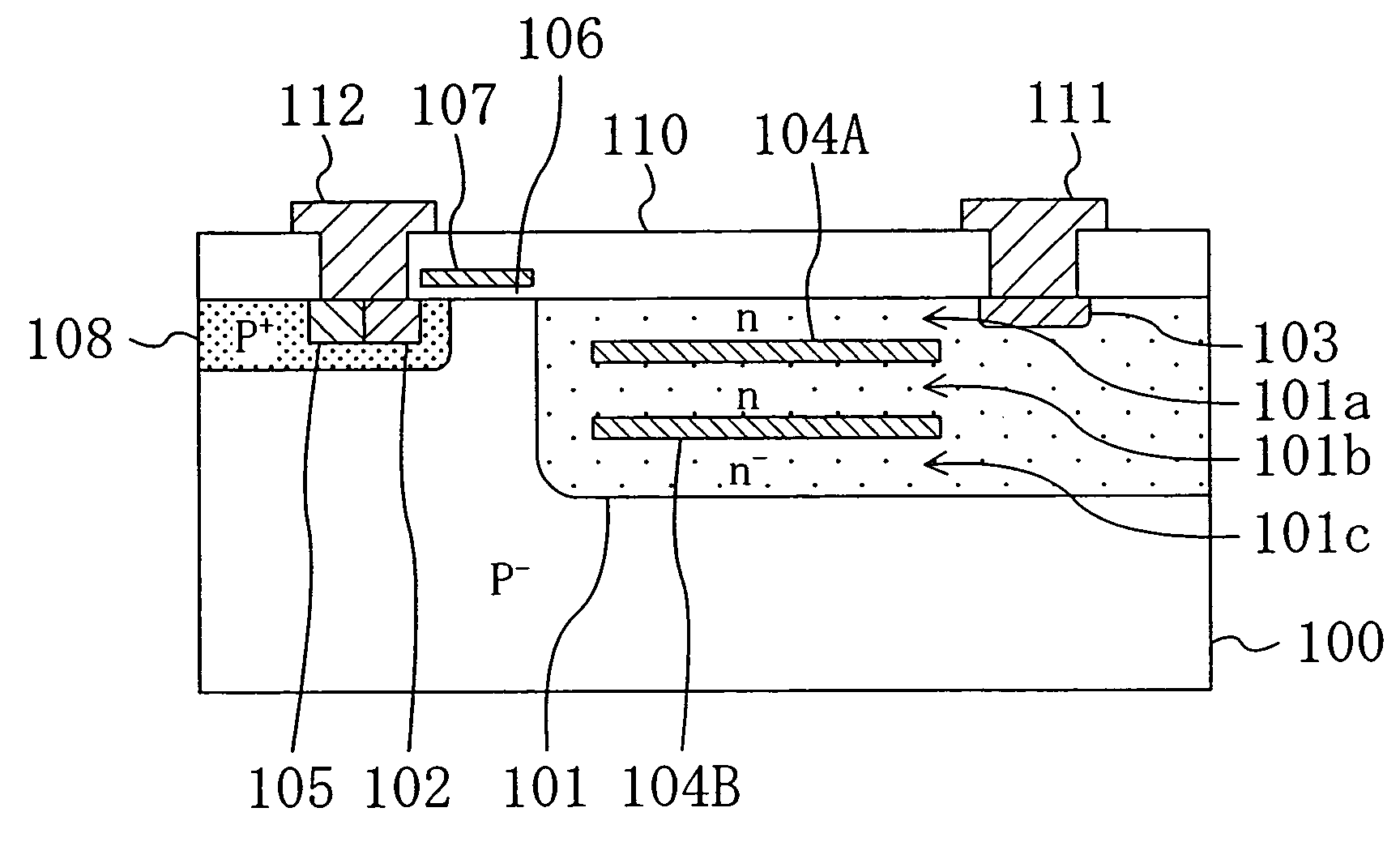
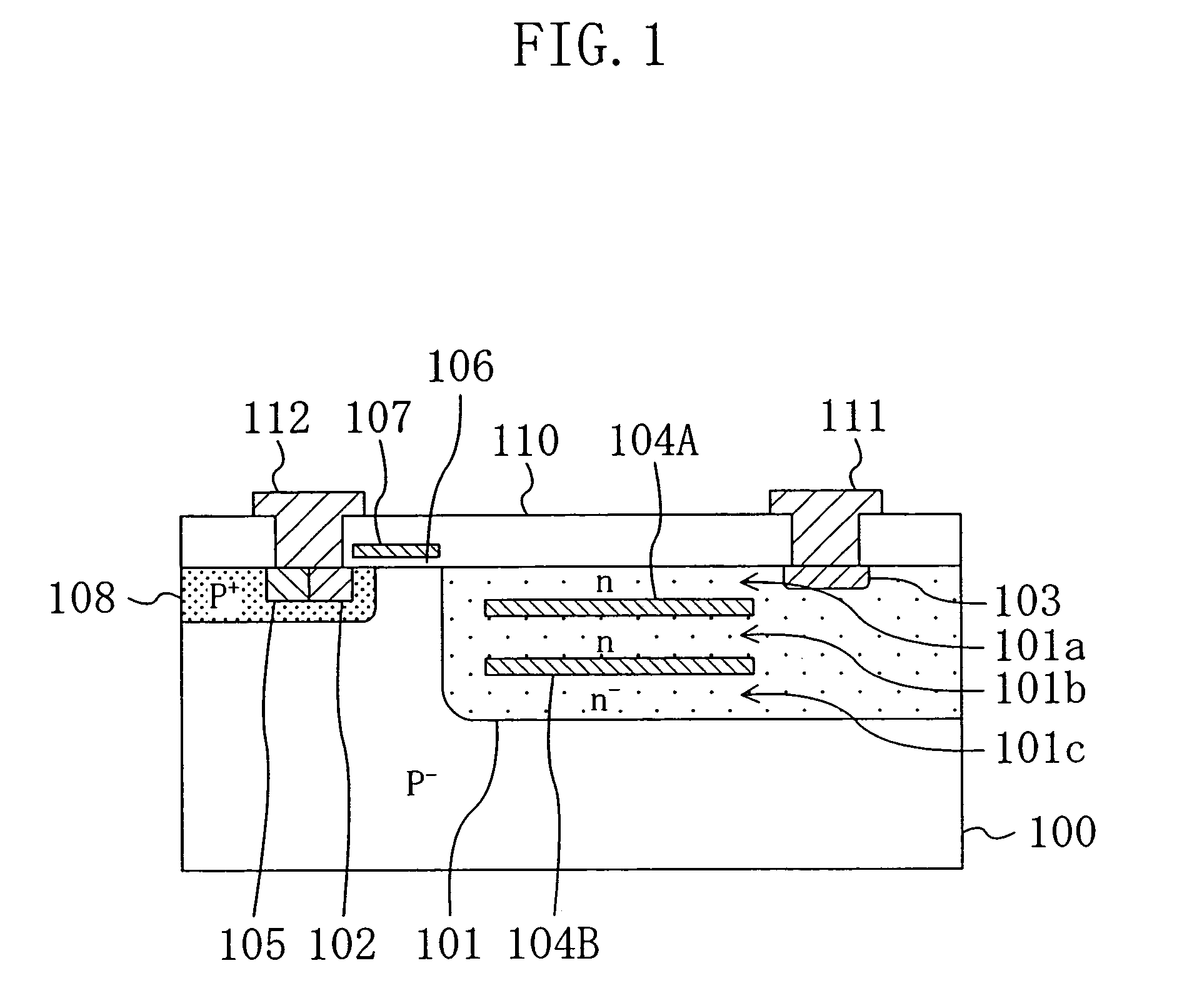
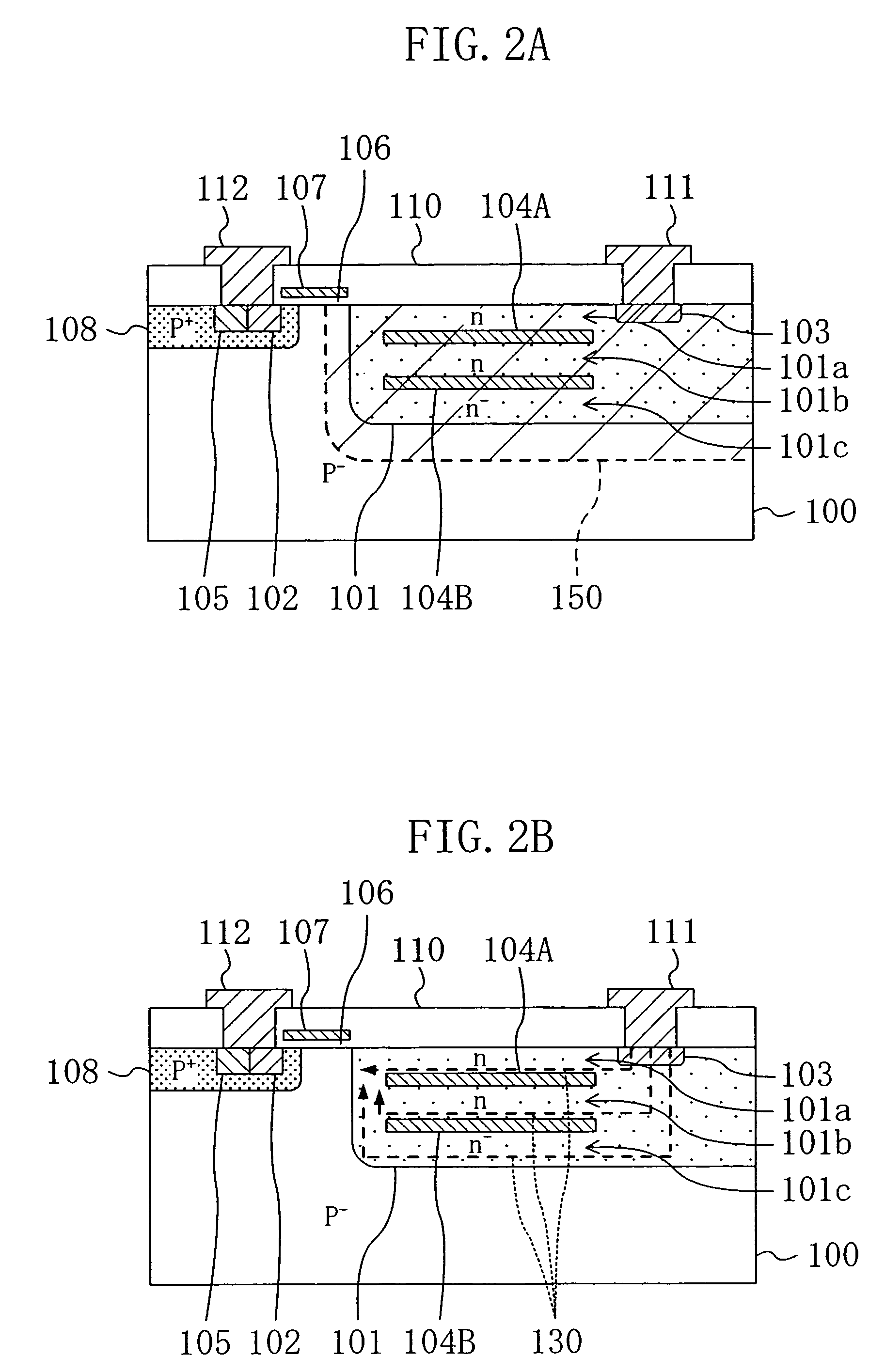
[0046]FIG. 1 is a cross-sectional view illustrating a semiconductor device, which is a high-voltage MOS transistor, according to the embodiment of the present invention.

[0047]As illustrated in FIG. 1, the semiconductor device includes a semiconductor substrate 100 made of silicon whose p-type impurity concentration is about 1×10¹⁴ / cm3 to about 3×10¹⁴ / cm3. An n-type extended drain region 101 and an n-type source region 102 are formed with an interval therebetween in an upper portion of the semiconductor substrate 100. In an upper portion of the extended drain region 101, a drain contact portion 103 is formed. The drain contact portion 103 is electrically connected, via a contact section, to a drain electrode 111 formed on an insulating film 110.

[0048]The extended drain region 101 is formed by implantation of an n-type impurity with a very high implantation energy of about 1.0 MeV to abou...


PUM


Abstract

A semiconductor device includes a semiconductor substrate of a first conductivity type, in which an extended drain region of a second conductivity type and a source region of the second conductivity type are formed with an interval therebetween, wherein the extended drain region includes a plurality of buried layers, each formed by burying an impurity layer of the first conductivity type, the plurality of buried layers extending substantially parallel to a substrate surface and with an interval therebetween in a depth direction. A concentration of an impurity of the second conductivity type in the extended drain region at a depth of about 6 μm from the substrate surface is about 1×10¹⁵/cm3 or more and is about 30% or more of that at a depth of about 2 μm from the substrate surface.

Description

[0001]This application is a divisional of application Ser. No. 10 / 307,361, filed Dec. 2, 2002, now abn.BACKGROUND OF THE INVENTION[0002]The present invention relates to a semiconductor device having a high breakdown voltage and a method for manufacturing the same.[0003]Various structures have been studied in the prior art for a lateral semiconductor device with which the on-state resistance can be reduced while ensuring a high breakdown voltage. An example of such a semiconductor device is disclosed in U.S. Pat. No. 6,168,983, which will now be described with reference to the drawings.[0004]FIG. 10 is a cross-sectional view illustrating a first semiconductor device disclosed in the U.S. patent.[0005]As illustrated in FIG. 10, an n-type source region 14 and an n-type extended drain region 23 are formed with an interval therebetween in an upper portion of a p-type semiconductor substrate 16. A drain contact portion 19 electrically connected to a drain electrode 11 is formed in an uppe...

Claims


Application Information

Patent Timeline
IPC IPC(8): H01L21/425H01L21/265H01L29/06H01L29/08H01L29/78
CPCH01L29/0634H01L29/7835H01L29/0847
Inventor UNO, TOSHIHIKO
Owner PANASONIC CORP
Why Eureka
Try Eureka