

Insulated gate field effect transistor and a method of manufacturing the same
- Summary
- Abstract
- Description
- Claims
- Application Information
AI Technical Summary
Benefits of technology
Problems solved by technology
Method used
Image

Examples
embodiment 1
[0084]Embodiment 1 relates to an insulated gate field effect transistor and a method of manufacturing the same.
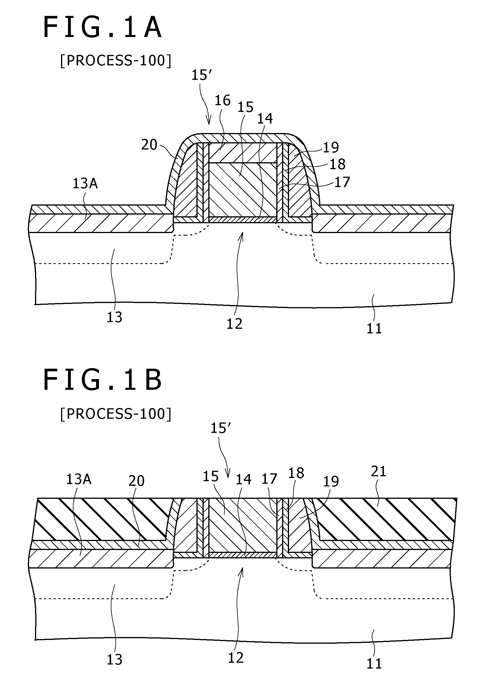
[0085]As shown in the form of a schematically partial end view in FIG. 1O, the insulated gate field effect transistor of Embodiment 1 is one including:
[0086](A) a source / drain region 13 and a channel formation region 12;
[0087](B) a gate electrode 23 formed above the channel formation region 12; and
[0088](C) a gate insulating film 30.
[0089]It is to be noted that in Embodiment 1, the insulated gate field effect transistor is set as n-channel one.
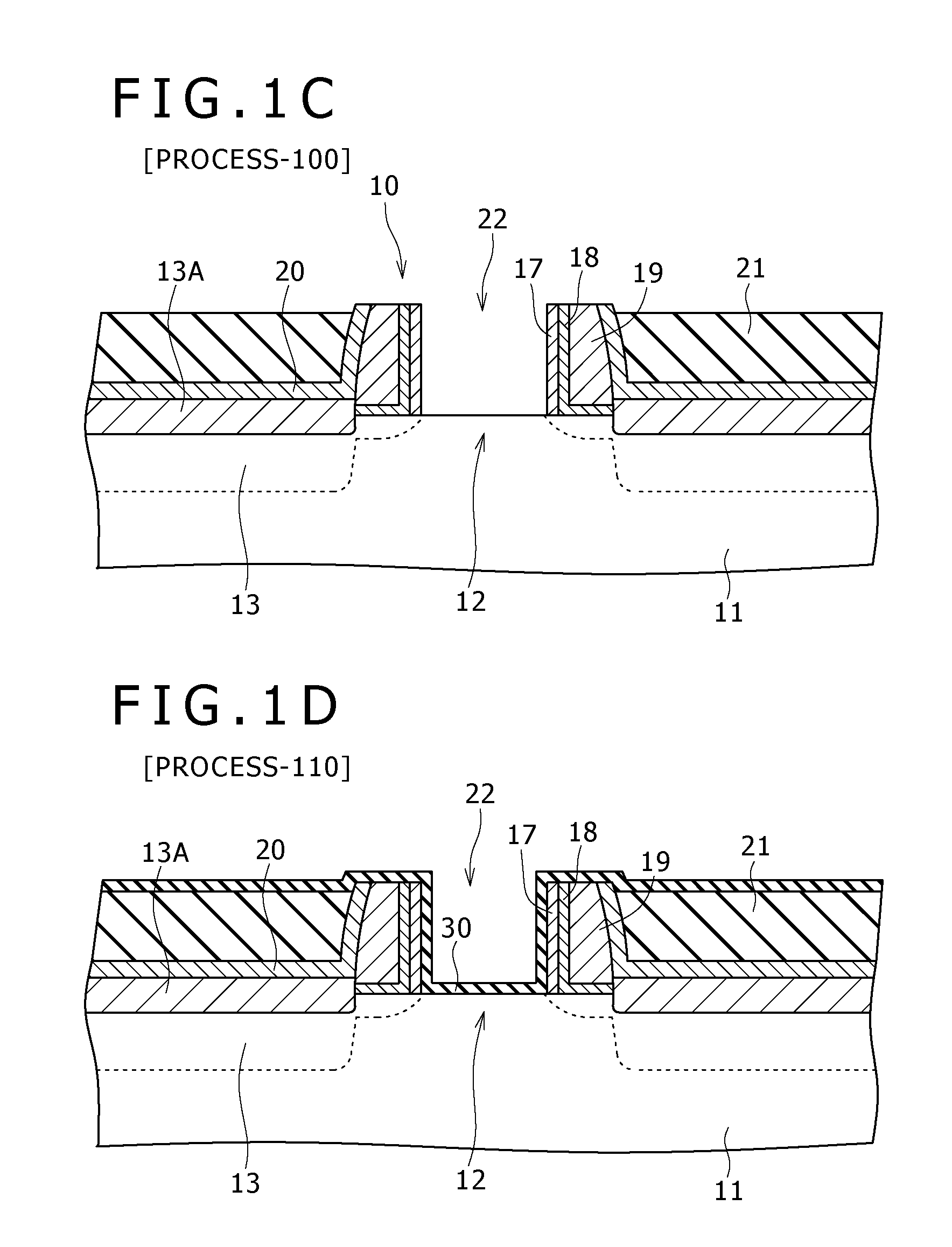
[0090]As shown in the form of a schematically enlarged cross sectional view in FIG. 1P, the gate insulating film 30 made of a hafnium oxide is composed of a gate insulating film main body portion 30A formed between the gate electrode 23 and the channel formation region 12, and a gate insulating film extension portion 30B extending from the gate insulating film main body portion 30A to a middle of a side surface portion 23A of the gate...
embodiment 2
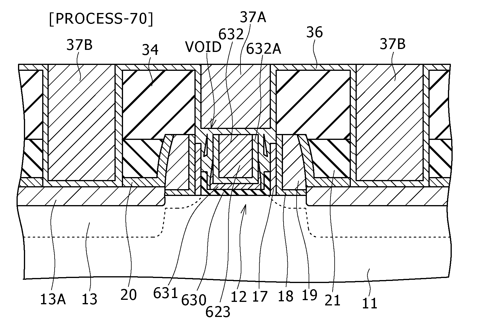
[0135]Embodiment 2 is a change of Embodiment 1. Specifically, Embodiment 2 relates to a method of manufacturing an insulated gate field effect transistor.
[0136]Although Embodiment 2 is identical to Embodiment 1 in that the first layer 31 is made of hafnium silicide (HfSix), Embodiment 2 is different from Embodiment 1 in that a second layer 232 is made of nickel silicide. In addition, Embodiment 2 is different from Embodiment 1 in a method of forming the second layer 232. Hereinafter, a method of manufacturing an insulated gate field effect transistor of Embodiment 2 will be described in detail with reference to FIGS. 2A to 2C.
[0137][Process-200]
[0138]Firstly, the same processes as those of [Process-100] to [Process-130] of Embodiment 1 are carried out.
[0139][Process-210]
[0140]After that time, a metallic material is filled in the remaining portion of the opening portion 22 for gate electrode formation by utilizing the following method. That is to say, a conductive material layer 50 i...
embodiment 3
[0146]Embodiment 3 is a change of Embodiment 1. Specifically, Embodiment 3 relates to an insulated gate field effect transistor, and a method of manufacturing the same.
[0147]Embodiment 3 is different from Embodiment 1 in that the entire gate electrode 323 is made of a nickel silicide 332. In addition, Embodiment 3 is also different from Embodiment 1 in a method of forming the gate electrode 323. Hereinafter, a method of manufacturing an insulated gate field effect transistor of Embodiment 3 will be described in detail with reference to FIGS. 3A to 3D.
[0148][Process-300]
[0149]Firstly, the same processes as those of [Process-100] and [Process-110] of Embodiment 1 are carried out.
[0150][Process-310]
[0151]After that, the gate insulating film 30 formed on the sidewall of the opening portion 22 for gate electrode formation is selectively removed, thereby obtaining the gate insulating film 30 composed of the gate insulating film main body portion 30A and the gate insulating film extension ...
PUM
 Abstract
Description
Claims
Application Information