

Apparatus and method of fabricating thin film pattern
- Summary
- Abstract
- Description
- Claims
- Application Information
AI Technical Summary
Benefits of technology
Problems solved by technology
Method used
Image

Examples
Embodiment Construction
[0041]Reference will now be made in detail to the preferred embodiments of the invention, examples of which are illustrated in the accompanying drawings.
[0042]With reference to FIGS. 3 to 5, embodiments of the invention will be explained as follows.
[0043]A fabricating method and apparatus of a thin film pattern according to one preferred embodiment of the invention uses an etch resist solution that includes a surfactant inclusive of an ethylene oxide fluorinated polymer. The etch resist solution including this surfactant has a stronger adhesive force with the print plate than with the blanket, thus it becomes possible to easily transfer the etch resist solution from the blanket to the print plate. As a result, the reliability of forming the thin film pattern by a resist printing method can be improved.
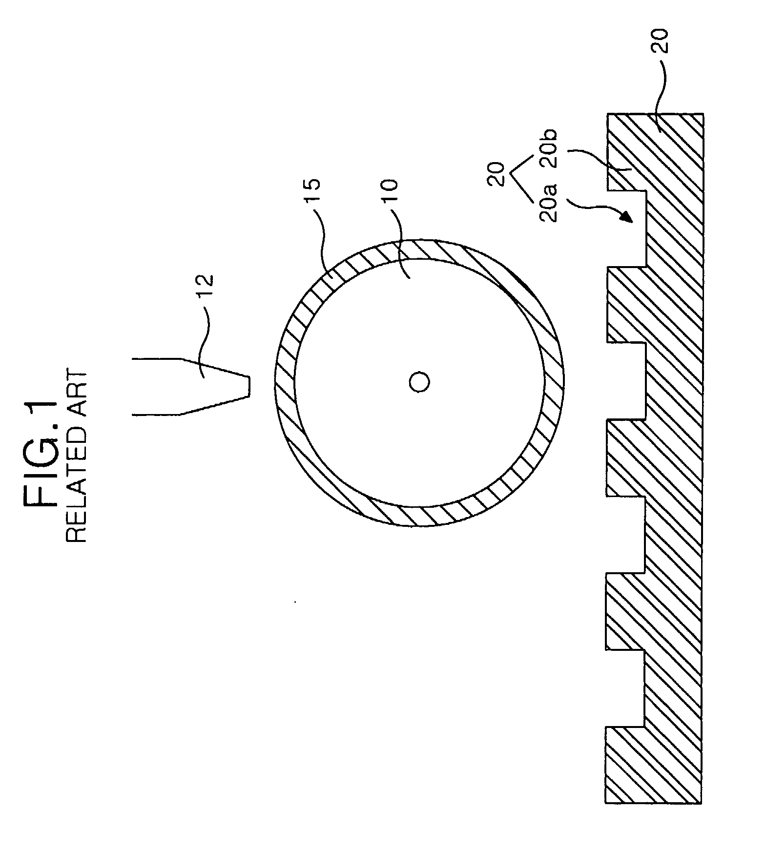
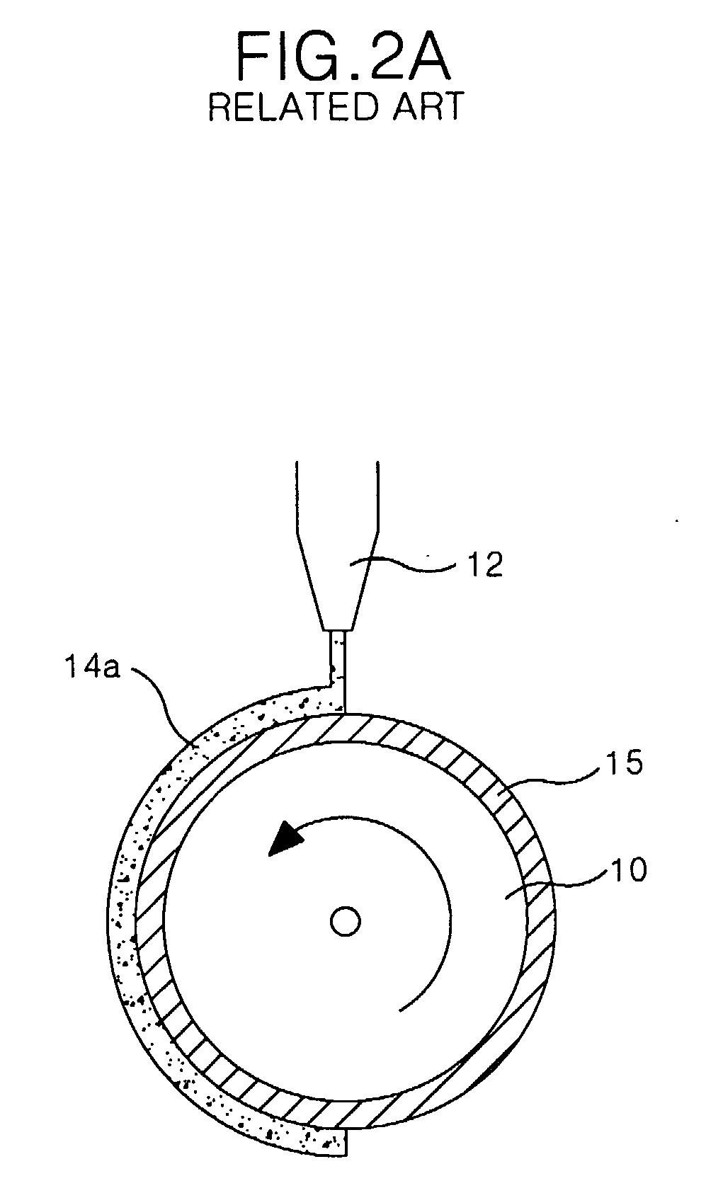
[0044]Referring to FIGS. 2A to 2D, the etch resist solution of the invention will be explained in detail in conjunction with a fabricating method of a thin film pattern by a resist pri...
PUM
| Property | Measurement | Unit |
|---|---|---|
| Fraction | aaaaa | aaaaa |
| Fraction | aaaaa | aaaaa |
| Fraction | aaaaa | aaaaa |
Abstract
Description
Claims
Application Information