Active filter circuit with reduced noise

a filter circuit and active technology, applied in the field of filter circuits, can solve the problems of inability to adjust the variations in temperature characteristics and device values, and the voltage controlled current source itself can become a main noise source, and achieve the effect of reducing the noise of input conversion

Inactive Publication Date: 2006-03-07
LAPIS SEMICON CO LTD
View PDF6 Cites 9 Cited by
  • Summary
  • Abstract
  • Description
  • Claims
  • Application Information

AI Technical Summary

Benefits of technology

[0033]It is an object of the invention to provide an active filter circuit which can reduce input conversion noises without causing a change in frequency band characteristics.

Problems solved by technology

That is, the resistors are generally formed with variations in temperature characteristics and device values upon manufacturing of the ICs and, after the ICs were once manufactured, it is impossible to adjust the variations in the temperature characteristics and device values.
Generally, since any devices (active device and passive device) generate noises, in the circuit obtained as a result of the above replacement, the voltage controlled current source itself can become a main noise source.

Method used


Image

  • Active filter circuit with reduced noise
  • Active filter circuit with reduced noise
  • Active filter circuit with reduced noise

Examples


second embodiment

(B) Second Embodiment

[0094]Only different points between the first and second embodiments will now be described hereinbelow.

[0095]The second embodiment will be also explained with respect to a filter circuit of the LC ladder type of the ternary π type as an example.

(B-1) Construction of the Second Embodiment

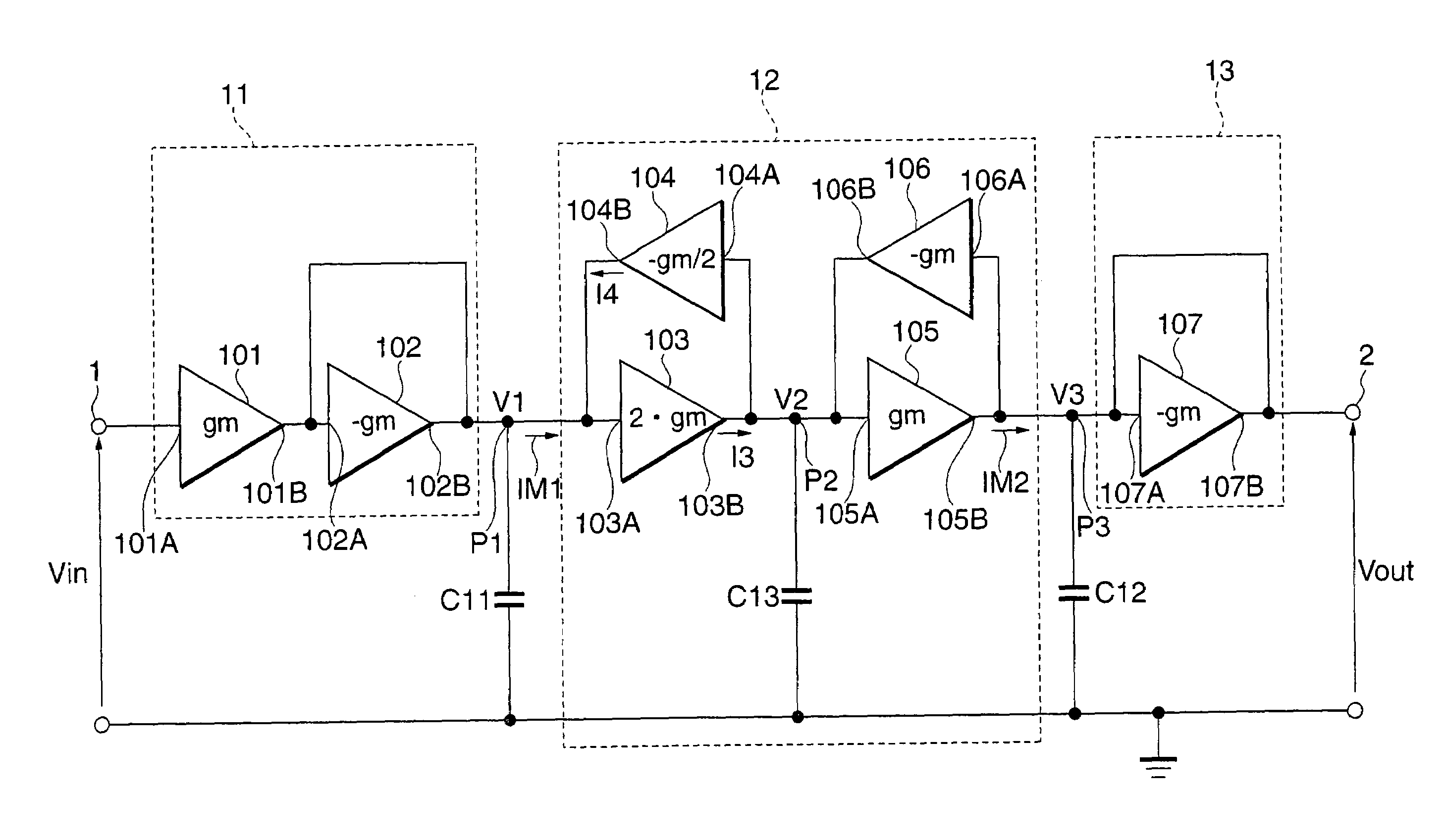
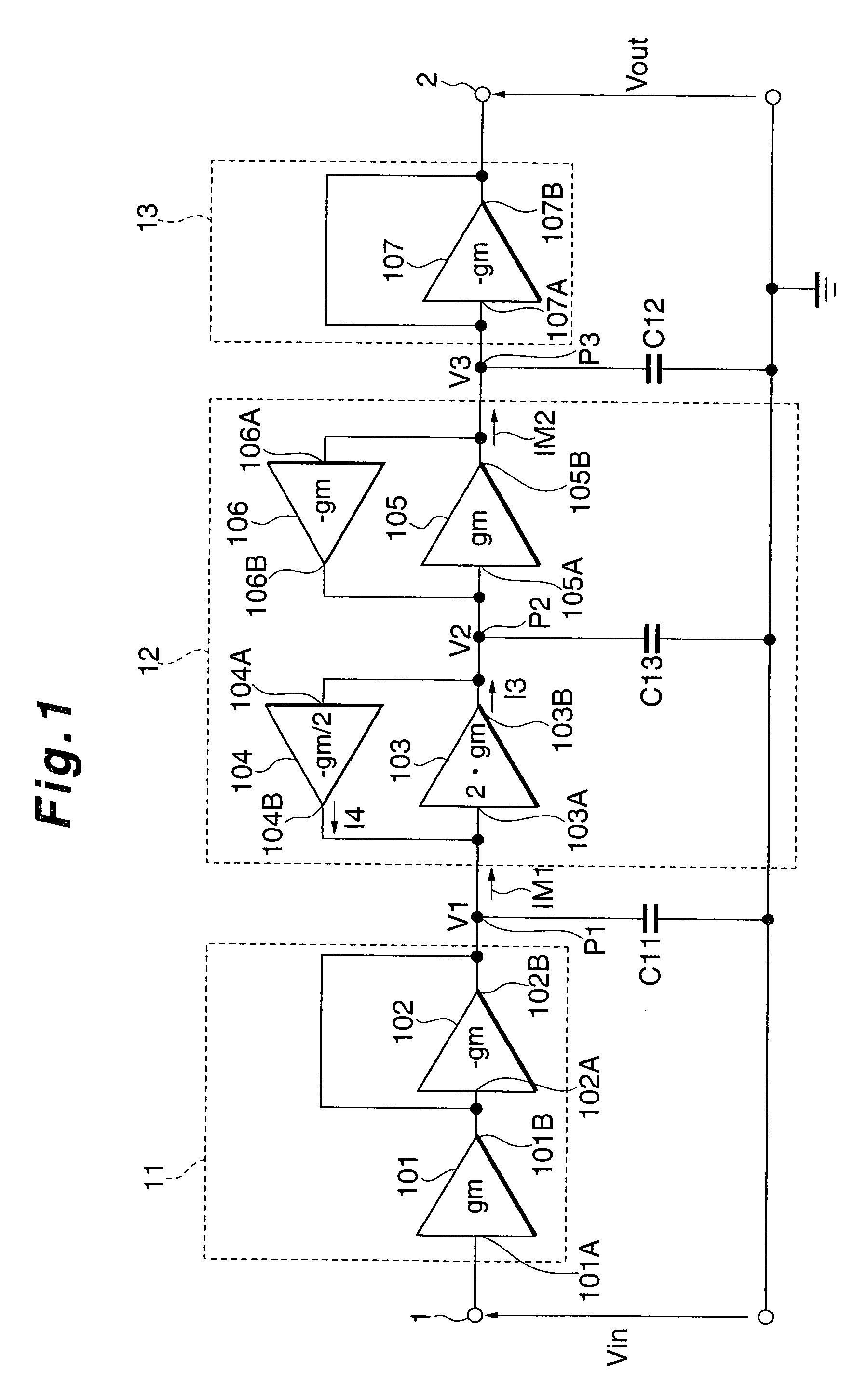
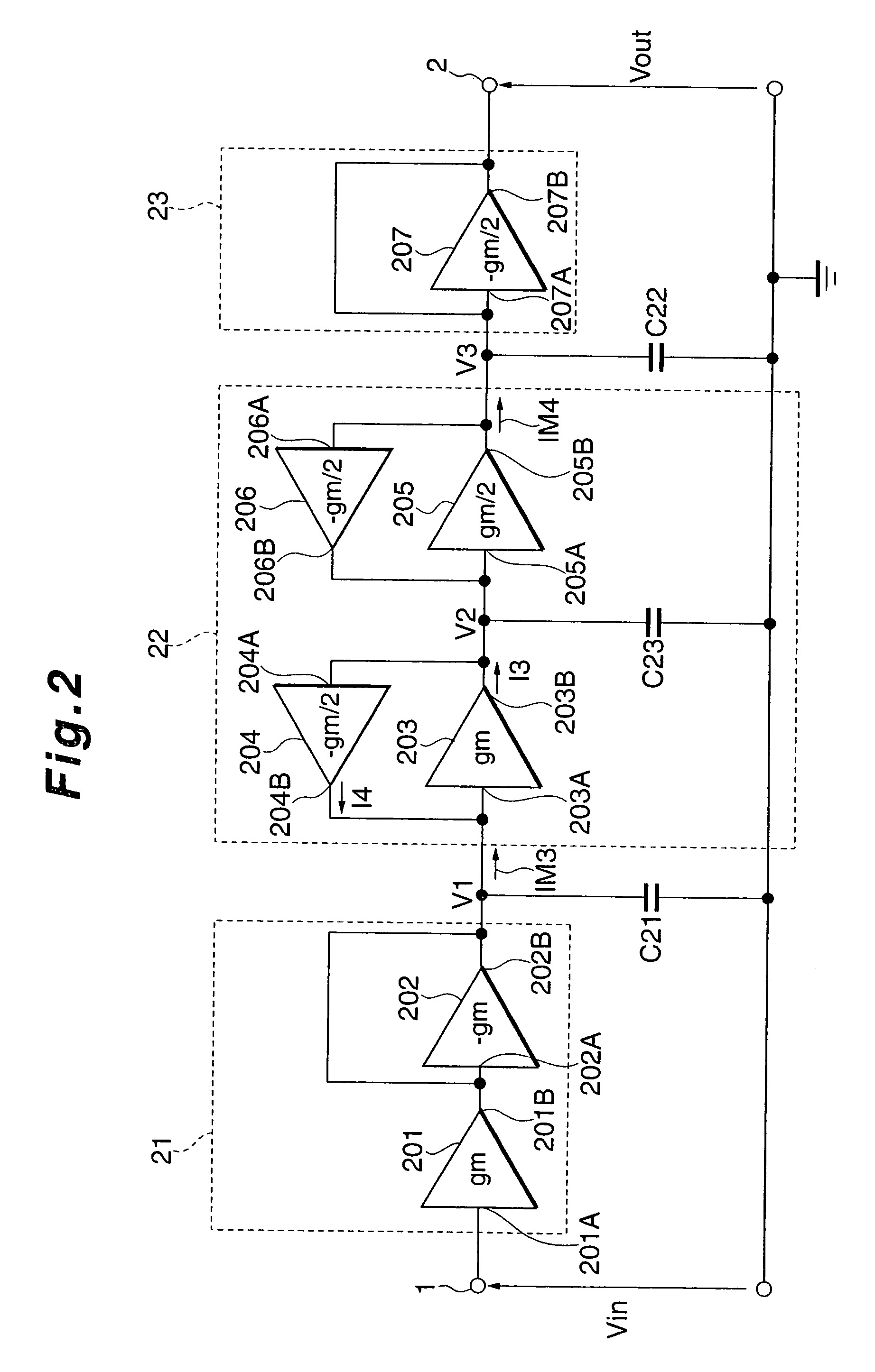
[0096]FIG. 2 shows the filter circuit of the second embodiment.

[0097]In FIG. 2, the filter circuit has the input terminal 1, the output terminal 2, an input terminating portion 21, an inductor portion 22, and an output terminating portion 23.

[0098]Voltage controlled current sources 201 to 207 constructing the portions 21 to 23 are provided in the filter circuit. Mutual conductances of the voltage controlled current sources 201 to 207 are set as follows. That is, the current sources 201 and 203 are set to gm, the current source 202 is set to −gm, the current source 205 is set to gm / 2, and the current sources 204, 206, and 207 are set to −gm / 2, respectively.

[0099]The input terminal...

third embodiment

(C) Third Embodiment

[0115]Only different points between the first embodiment and the third embodiment will be described hereinbelow.

[0116]Although the first embodiment has been described with respect to the filter circuit of the LC ladder type of the ternary π type, the third embodiment relates to a low pass filter circuit of the resistance both-terminating LC ladder type of the quinary π type.

(C-1) Construction of the Third Embodiment

[0117]FIG. 3 shows the filter circuit of the third embodiment.

[0118]In FIG. 3, the filter circuit has the input terminal 1, the output terminal 2, eleven voltage controlled current sources 301 to 311, and five capacitors C31 to C35.

[0119]Mutual conductances of the voltage controlled current sources 301 to 311 are set as follows. That is, the current sources 301, 303, 305, and 309 are set to gm, the current sources 302, 304, 306, 310, and 311 are set to −gm, the current source 307 is set to 5≅gm, and the current source 308 is set to −gm / 5, respectively....

fourth embodiment

(D) Fourth Embodiment

[0138]Only different points between the first and second embodiments and the fourth embodiment will now be described hereinbelow.

[0139]The fourth embodiment relates to a modification of the filter circuit 70.

(D-1) Construction and Operation of the Fourth Embodiment

[0140]FIG. 12 shows a filter circuit in the fourth embodiment.

[0141]In FIG. 12, the filter circuit has the input terminal 1, the output terminal 2, the input terminating portion 11, an intermediate circuit portion 80, and the output terminating portion 23.

[0142]Among them, the functions of the component elements designated by the same reference numerals as 1, 2, 11, and 23 in the first and second embodiments are substantially the same as those of the corresponding component elements in the first and second embodiments.

[0143]Therefore, the fourth embodiment is characterized by the intermediate circuit portion 80.

[0144]The intermediate circuit portion 80 has the voltage controlled current sources 103, 10...


PUM


Abstract

Input conversion noises of a filter circuit are reduced. The circuit has plural circuit arrangements obtained by dividing the filter circuit so as to include at least one voltage controlled current source, and at least one circuit arrangement is an amplification circuit having an amplifying function for amplifying an input signal to the filter circuit at a set amplification factor. The amplification element circuit has: a loop circuit constructed by plural intra-loop voltage controlled current sources in which mutual conductance values have a predetermined corresponding relation; and a corresponding capacitor connected to a node in the loop circuit and having a capacitance depending on the corresponding relation so as to set a potential at the node to a predetermined potential corresponding to the amplification factor, and amplification element circuit has an electric nature which is independent of the amplification factor when seeing from the input side of the filter circuit.

Description

BACKGROUND OF THE INVENTION[0001]1. Field of the Invention[0002]The invention relates to a filter circuit which is suitable when it is applied to, for example, an integrated circuit or the like.[0003]2. Related Background Art[0004]There are the following reference literatures 1 to 3 as literatures describing conventional analog filter circuits.[0005]Reference literature 1: JP-A-6-120772[0006]Reference literature 2: JP-A-6-164314[0007]Reference literature 3: JP-A-11-004139[0008]Among them, it is an object of the reference literature 1 to provide an active filter in which an amplitude range of an input signal is widened while suppressing an increase in current consumption.[0009]It is an object of an active filter circuit of the reference literature 2 to improve an S / N ratio of the filter circuit and suppress input conversion noises.[0010]It is an object of an active filter circuit of the reference literature 3 that, in a filter circuit of the LC ladder type constructed by a voltage co...

Claims


Application Information

Patent Timeline
Patent Type & Authority Patents(United States)
IPC IPC(8): H03B1/00H03H11/04H03H11/12H03H11/48
CPCH03H11/0444
Inventor YOSHIDA, YOSHIKAZUYOSHIDA, AKIRA
Owner LAPIS SEMICON CO LTD
Why Eureka
Try Eureka