OLEDs having increased external electroluminescence quantum efficiencies

a technology of external electroluminescence and quantum efficiency, which is applied in the direction of discharge tube/lamp details, organic semiconductor devices, discharge tube luminescnet screens, etc., can solve the problems of limiting the practical application of oleds, their susceptibility to environmental elements, and the luminescence or brightness in directions extending outwardly from the surface of the device is reduced, so as to increase the out-coupling efficiency, and increase the out-coup

Inactive Publication Date: 2006-03-14
UNIVERSAL DISPLAY
View PDF28 Cites 114 Cited by
  • Summary
  • Abstract
  • Description
  • Claims
  • Application Information

AI Technical Summary

Problems solved by technology

These phenomena result in decreased external electroluminescence quantum efficiency and a reduction in the luminescence or brightness in directions extending outwardly from the surface of the device.
Another factor limiting the practical application of OLEDs is their susceptibility to environmental elements such as moisture and oxygen.
Oxygen and moisture can produce deleterious effects on certain OLED structural components, such as reactive metal cathode components.
Without protection, the lifetime of the devices can be severely limited.
The organic materials utilized in a conventional OLED structure can also be adversely affected by environmental species such as water and oxygen.

Method used


Image

  • OLEDs having increased external electroluminescence quantum efficiencies
  • OLEDs having increased external electroluminescence quantum efficiencies
  • OLEDs having increased external electroluminescence quantum efficiencies

Examples


Embodiment Construction

[0022]The present invention now will be described more fully hereinafter with reference to the accompanying drawings in which preferred embodiments of the invention are shown. This invention may, however, be embodied in different forms and should not be construed as limited to the embodiments set forth herein.

[0023]As used herein, a “layer” of a given material includes a region of that material whose thickness is small compared to both its length and width. Examples of layers include sheets, foils, films, laminations, coatings, and so forth. As used herein a layer need not be planar, but can be bent, folded or otherwise contoured, for example, to at least partially envelop another component. As used herein a layer can also include multiple sub-layers. A layer can also consist of a collection of discrete portions, for example, a layer of discrete active regions comprising individual pixels.

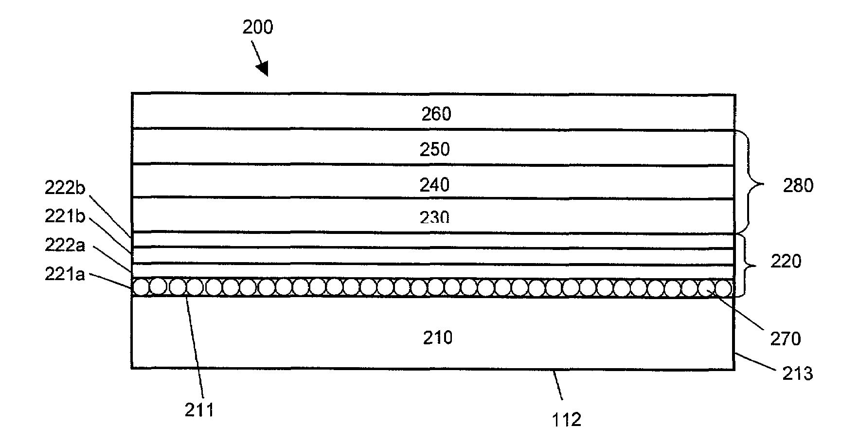
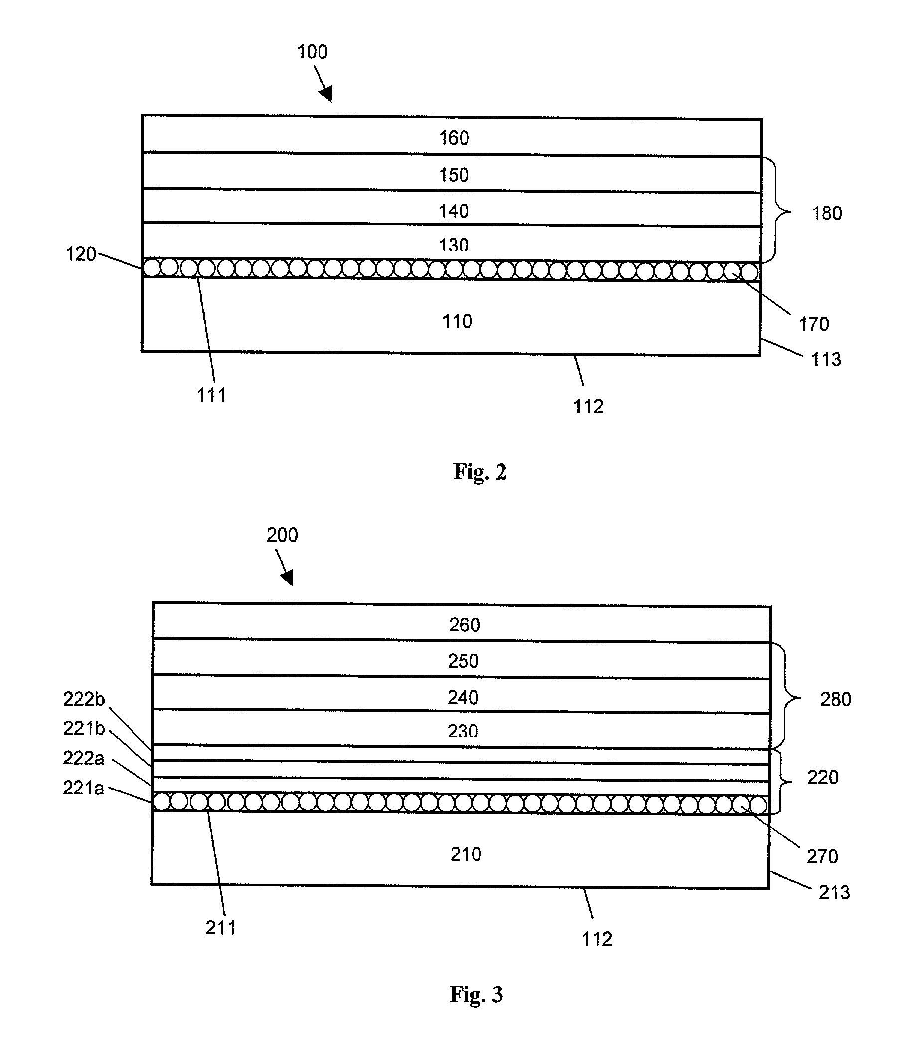
[0024]The present invention is directed to an OLED device comprising: (a) a substrate; (b) an a...


PUM


Abstract

OLED devices are disclosed having increased external electroluminescence quantum efficiencies, i.e., increased “out-coupling” efficiencies. OLED devices that have increased out-coupling efficiencies and that are also protected from environmental elements such as moisture and oxygen are also disclosed. The OLED device of the present invention comprises a substrate; an active region positioned on the substrate, wherein the active region comprises an anode layer, a cathode layer and a light-emitting layer disposed between the anode layer and the cathode layer; and a polymeric layer disposed (a) over the active region, (b) under the active region or (c) both over and under the active region. The polymeric layer has microparticles incorporated therein, and the microparticles are effective to increase the out-coupling efficiency of the OLED. In one embodiment, the OLED device comprises a composite barrier layer and the microparticles are incorporated in a polymeric planarizing sublayer of the composite barrier layer. The composite barrier layer in this embodiment also protects the OLED from damage caused by environmental elements such as moisture and / or oxygen.

Description

FIELD OF THE INVENTION[0001]The present invention relates to organic optoelectronic devices, more particularly to organic light emitting devices (OLEDs) having increased external electroluminescence (EL) quantum efficiencies or “out-coupling” efficiencies. OLEDs having increased out-coupling efficiencies and that are protected from environmental elements such as moisture and or oxygen are also disclosed.BACKGROUND OF THE INVENTION[0002]Organic light emitting devices (“OLEDs”), including both polymer and small-molecule OLEDs, are potential candidates for a great variety of virtual- and direct-view type displays, such as lap-top computers, televisions, digital watches, telephones, pagers, cellular telephones, calculators and the like. Unlike inorganic semiconductor light emitting devices, organic light emitting devices are generally simple and are relatively easy and inexpensive to fabricate. Also, OLEDs readily lend themselves to applications requiring a wide variety of colors and to...

Claims


Application Information

Patent Timeline
Patent Type & Authority Patents(United States)
IPC IPC(8): H05B33/00H01L51/52
CPCH01L51/5268H01L51/5256H01L51/5253H10K50/8445H10K50/854H10K2102/3031H10K50/844
Inventor WEAVER, MICHAEL STUARTBULOVIC, VLADIMIRLU, MIN-HAO MICHAEL
Owner UNIVERSAL DISPLAY
Why Eureka
Try Eureka