
Deterministically doped field-effect devices and methods of making same

a field-effect device and determinist-type technology, applied in the direction of semiconductor devices, electrical devices, nanotechnology, etc., can solve the problems of traditional stochastic approach to doping, inability and inability to use traditional diffusion or implantation techniques to control the atomic scale positioning of dopant atoms

Inactive Publication Date: 2006-03-21
ZH HANDOTAI KENKYU SHINKOKAI
View PDF23 Cites 127 Cited by
  • Summary
  • Abstract
  • Description
  • Claims
  • Application Information

AI Technical Summary

Benefits of technology

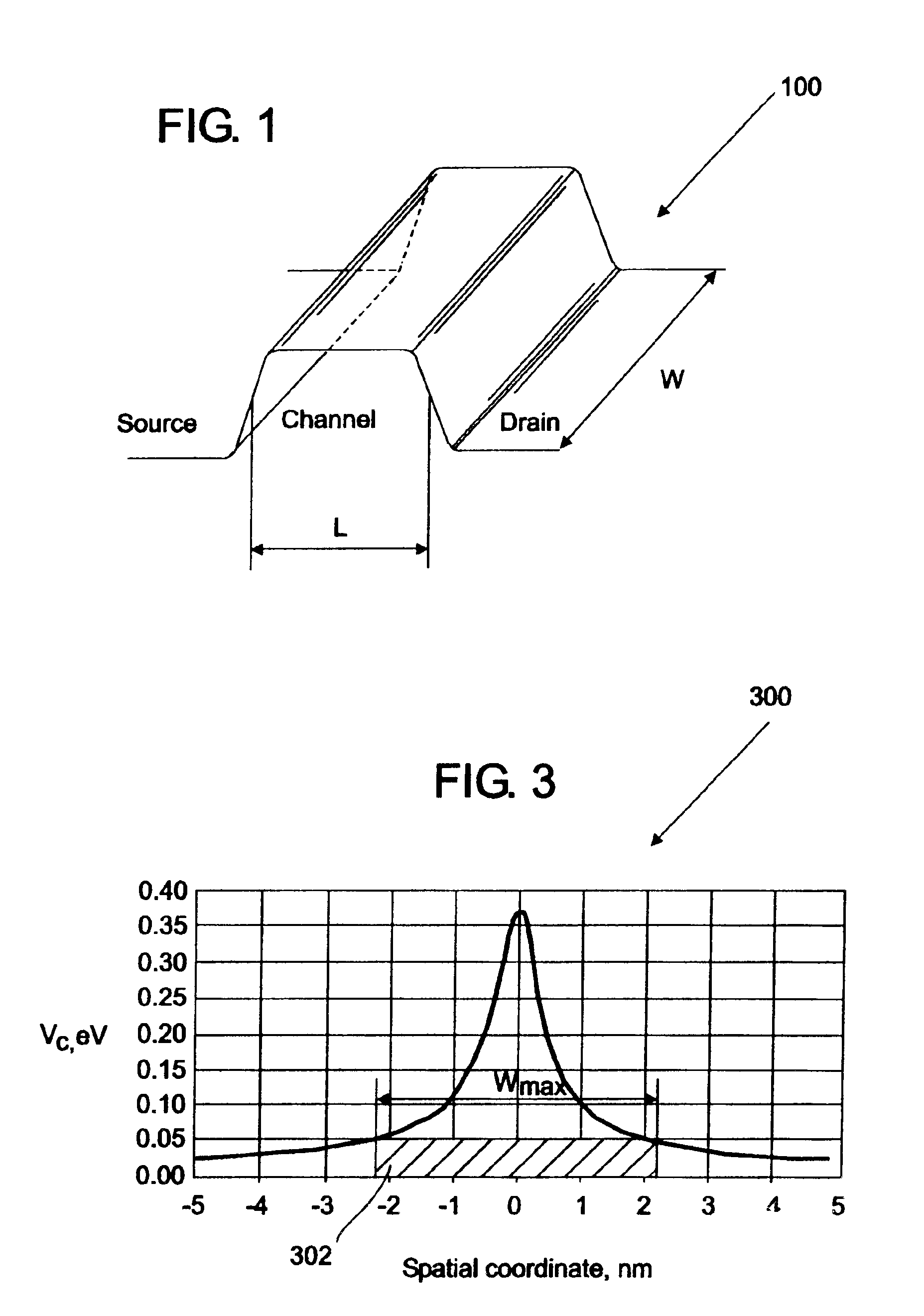
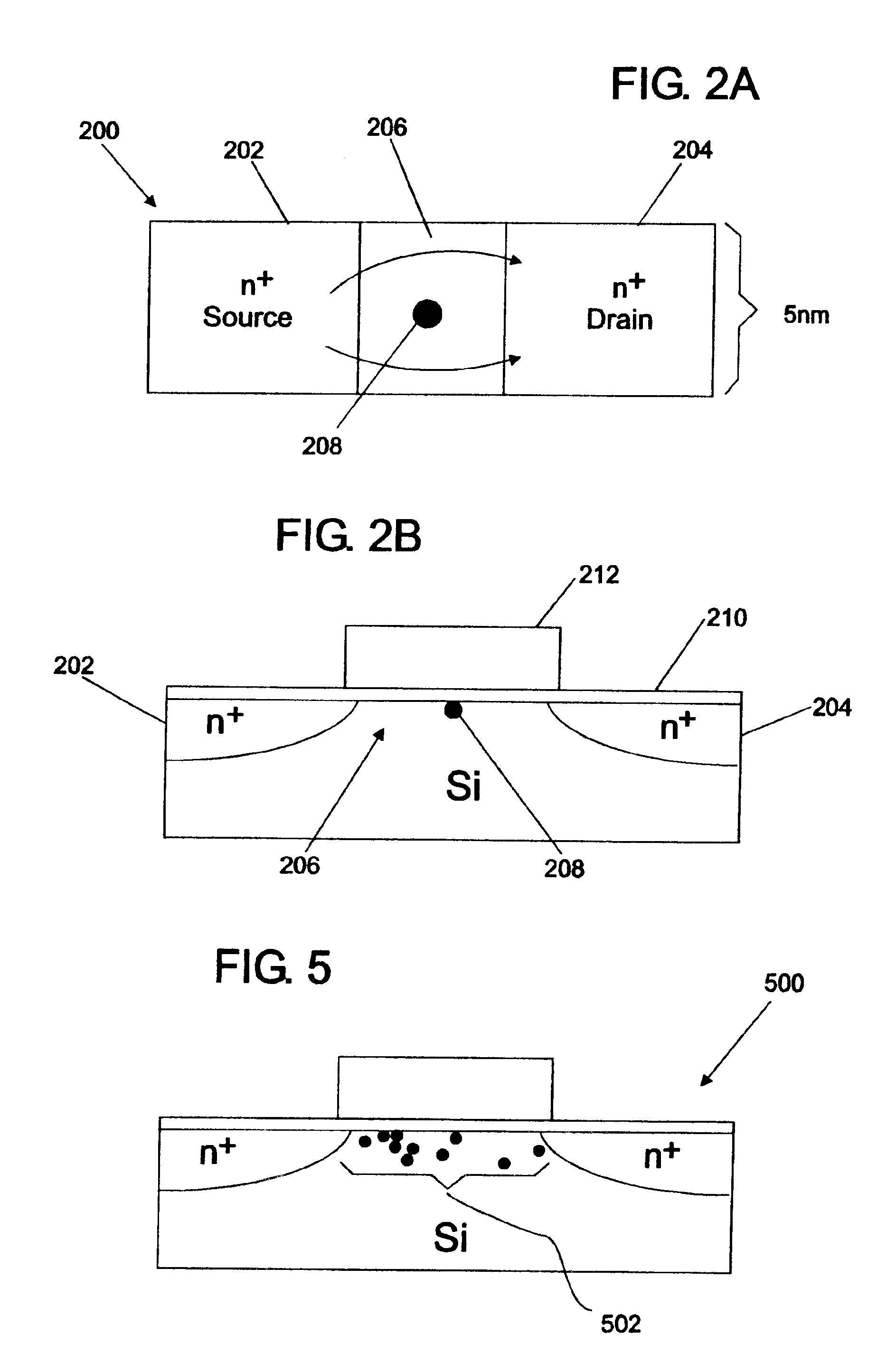
[0007]The present invention is directed to field-effect semiconductor devices and methods of making such devices where relatively small numbers of dopant atoms, also referred to as impurities or impurity atoms, are arranged in the channel in an engineered array or engineered arrays. An engineered array is defined as a configuration of one or more dopant atoms, where each atom is placed in a specific, predetermined location with respect to the channel and other dopant atom(s) in the channel. In this way, ultra-small devices with appropriate performance characteristics can be realized.
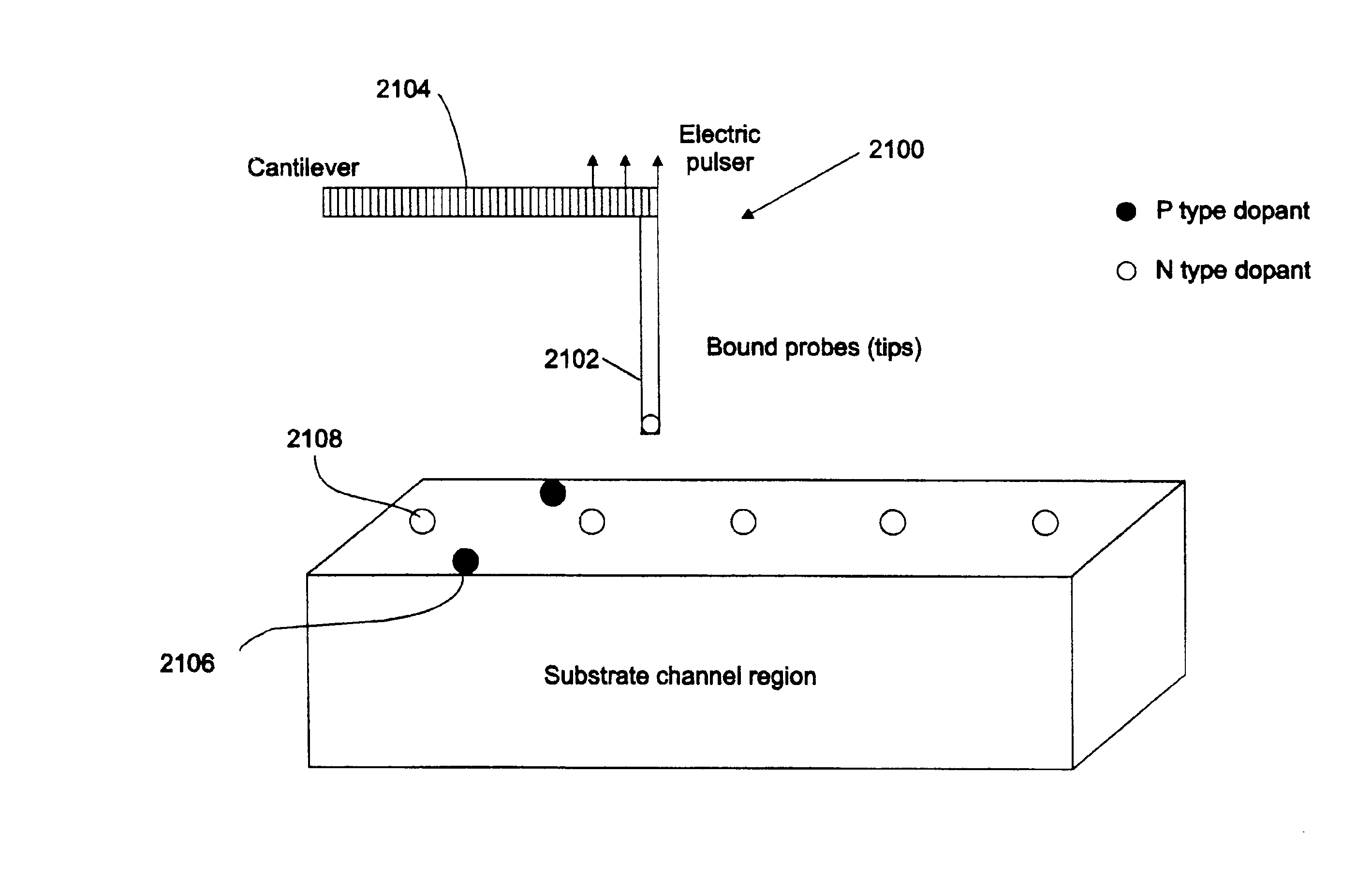
[0011]In another embodiment, such a transistor is formed by first forming a semiconductor substrate, and then placing a first atom of the engineered array of dopant atoms on the substrate. A first epitaxial film of depleted semiconductor material can then be grown over the first atom and the semiconductor substrate. A second atom of the engineered array of dopant atoms is then placed on the first epitaxial film, and a second epitaxial film is grown. Atoms and epitaxial films can then alternately be placed atop the structure until the engineered array of dopant atoms is formed beneath a final epitaxial film of depleted semiconductor material. A dielectric layer can then be applied, followed by patterning and the forming of a gate as before. Depending on the embodiment, atoms can be placed by proximity probe manipulation, ion implantation, or facilitating self-assembly of the atoms as necessary.

Problems solved by technology

However, conventional doping processes, such as traditional diffusion or implantation techniques, cannot be used to control the atomic scale positioning of dopant atoms.
As feature sizes are scaled to a few nanometers (nm), the traditional stochastic approach to doping is presenting problems.
However, large channel doping densities in such conventionally scaled FETs adversely decrease device performance, for example, due to multiple scattering that decreases channel mobility.
Hence, conventional stochastic doping technology limits the feasibility of achieving concurrent improvements in the performance of scaled, ultra-small FETs.
Such a small number of dopants in the thin surface layer cannot be obtained reproducibly using conventional doping techniques.
Taking into account the uncertainty in dopant position, in addition to the uncertainty in the number of dopants, will make the parameter variability even worse.
Uncertainty of the individual transistor's parameters in one chip imposes a practical limit to scaling, due to the difficulty of design, fabrication and operation of complex systems based on non-identical FETs.

Method used


Image

  • Deterministically doped field-effect devices and methods of making same
  • Deterministically doped field-effect devices and methods of making same
  • Deterministically doped field-effect devices and methods of making same

Examples


Embodiment Construction

[0035]The present invention will now be described in terms of specific, example embodiments. It is to be understood that the invention is not limited to the example embodiments disclosed. It should also be understood that not every feature of the semiconductor devices described is necessary to implement the invention as claimed in any particular one of the appended claims. Various elements and features of various embodiments of devices and processes are described to fully enable the invention. It should also be understood that throughout this disclosure, where a process or method is shown or described, the steps of the method may be performed in any order or simultaneously, unless it is clear from the context that one step depends on another being performed first.

[0036]At least some of the drawings, which are used to illustrate the inventive concepts, are not mutually exclusive. Rather, each one has been tailored to illustrate a specific concept discussed. In some cases, the element...


PUM


Abstract

Deterministically doped field-effect devices and methods of making same. One or more dopant atoms, also referred to as impurities or impurity atoms, are arranged in the channel region of a device in engineered arrays. Component atoms of an engineered array are substantially fixed by controlled placement in order to provide a barrier topology designed to control of source-drain carrier flow to realize an ultra-small device with appropriate, consistent performance characteristics. Devices can be made by placing atoms using proximity probe manipulation, ion implantation, by facilitating self-assembly of the atoms as necessary, or other techniques. These atomic placement techniques are combined in example embodiments with traditional methods of forming a substrate, insulators, gates, and any other structural elements needed in order to produce practical field-effect devices.

Description

CROSS REFERENCE TO RELATED APPLICATIONS[0001]This application is a continuation-in-part of and claims priority from commonly owned, U.S. application Ser. No. 09 / 510,802, filed Feb. 23, 2000, now U.S. Pat. No. 6,664,559 the entire disclosure of which is incorporated herein by reference. This application claims priority from commonly owned, U.S. Provisional Application Ser. No. 60 / 407,542, filed Aug. 30, 2002, the entire disclosure of which is incorporated herein by reference.BACKGROUND OF INVENTION[0002]Conventional semiconductor doping is not a deterministic process, i.e. it creates a statistical distribution of dopants. In the case of field-effect devices, stochastic doping enables reliable device performance by ensuring a reproducible distribution of large numbers of dopant atoms in the channel region. However, conventional doping processes, such as traditional diffusion or implantation techniques, cannot be used to control the atomic scale positioning of dopant atoms. In conventi...

Claims


Application Information

Patent Timeline
Patent Type & Authority Patents(United States)
IPC IPC(8): H01L31/119H01L21/22H01L29/10H01L29/12H01L29/16H01L29/167H01L29/36H01L29/76H01L29/78
CPCB82Y10/00H01L21/221H01L29/1033H01L29/12H01L29/16H01L29/167H01L29/36H01L29/1602Y10S977/938H01L29/7613H01L29/786
Inventor HERR, DANIEL JOSEPH CHRISTIANZHIRNOV, VICTOR VLADIMIROVICH
Owner ZH HANDOTAI KENKYU SHINKOKAI
Learn More