Plasma display panel device

a technology of display panel and plasma, which is applied in the direction of instruments, discharge tubes luminescnet screens, and electrodes, etc., can solve the problems of difficult high-definition display of images, inability to achieve uniform light emission for display, and increase in costs, so as to achieve easy high-definition image display, reduce electromagnetic radiation, and uniform light emission

Inactive Publication Date: 2006-03-21
PIONEER CORP
View PDF5 Cites 3 Cited by
  • Summary
  • Abstract
  • Description
  • Claims
  • Application Information

AI Technical Summary

Benefits of technology

[0019]In view of the above, it is an object of the present invention to provide a PDP device capable of obtaining a uniform state of light emission for displaying and of reducing electromagnetic radiation while easily achieving a high-definition image display.
[0037]With the above configurations, each of scanning electrodes and each of common electrodes making up a pair of row electrodes that provides one display row, are formed, in parallel with a row direction on a face of a front substrate facing a rear substrate and a folding-back electrode is formed on either of the common electrode or scanning electrode, and therefore the scanning electrode and the common electrode can be drawn out from a same direction of a PDP panel for at least every one display row, which can cancel magnetic flux occurring in a unit of a display row. Therefore, it is possible to obtain a uniform state of light emission for displaying and to reduce electromagnetic radiation while easily achieving a high-definition image display.

Problems solved by technology

However, since a thin configuration of a PDP device is its prime selling point, such the electromagnetic shield not only hinders the thin configuration but also causes an increase in costs.
First, in the first conventional technology, each of a plurality of display cells in which the scanning electrode 101 and the common electrode 102 are formed has a different impedance in every display cell due to a difference in the drawing-out position 109 on the left side of the panel caused by a positional variation in a row direction H. Therefore, since light-emitting luminance and / or controlled state are made different in every display cell, a uniform state of light emission for displaying cannot be achieved.
Therefore, since same scanning electrodes or same electrodes can always display same contents only, high-definition display of an image becomes difficult.
To solve this problem, a method may be available in which address electrodes are separated depending on either of an odd row or an even row, however, to achieve this, a very complicated driving circuit is required, which inescapably causes very high manufacturing costs.

Method used


Image

  • Plasma display panel device
  • Plasma display panel device
  • Plasma display panel device

Examples


first embodiment

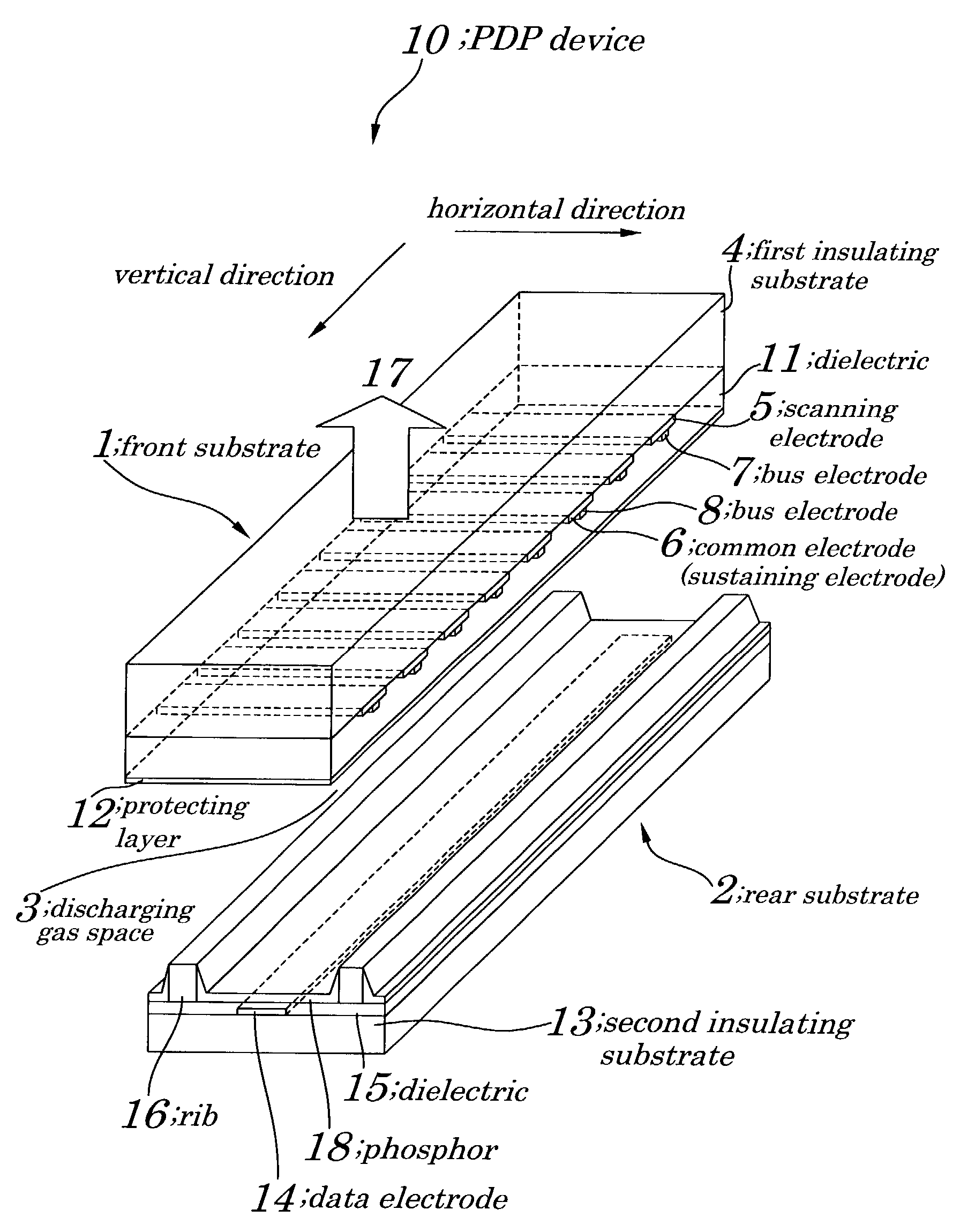
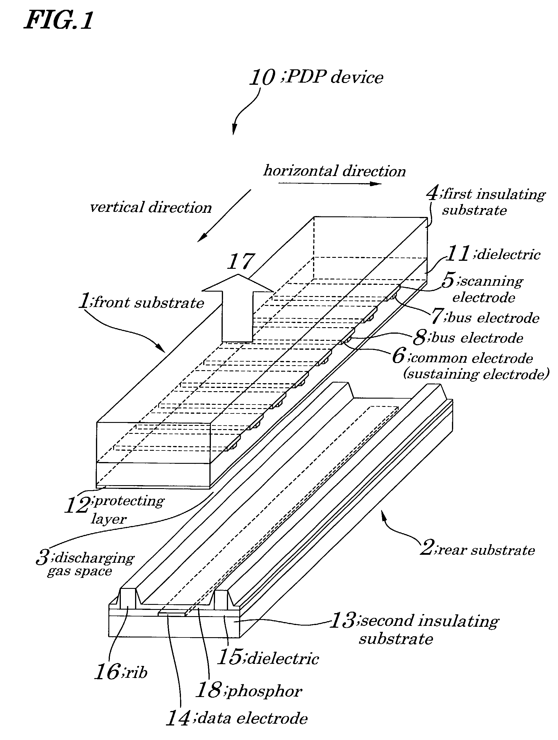
[0052]FIG. 1 is a perspective view showing configurations of a PDP device 10 of a first embodiment. FIG. 2 is a plan view showing configurations of main components of the PDP device 10 of the first embodiment. FIG. 3 is a schematic cross-sectional view illustrating a method for driving the PDP device 10 of the first embodiment. The PDP device 10 of the first embodiment, as shown in FIG. 1, has a basic configuration in which discharge gas space 3 is formed between a front substrate 1 and a rear substrate 2. The front substrate 1 includes a first insulating substrate 4 made from glass or a like, a scanning electrode 5 and a common electrode (sustaining electrode) 6 each being made from a transparent conductor such as ITO (Indium Tin Oxide) or a like and being formed on the first insulating substrate 4 in parallel with each other so as to form a pair of the scanning electrode 5 and the common electrode 6 in a horizontal direction H and to make up one display row (line), bus electrodes ...

second embodiment

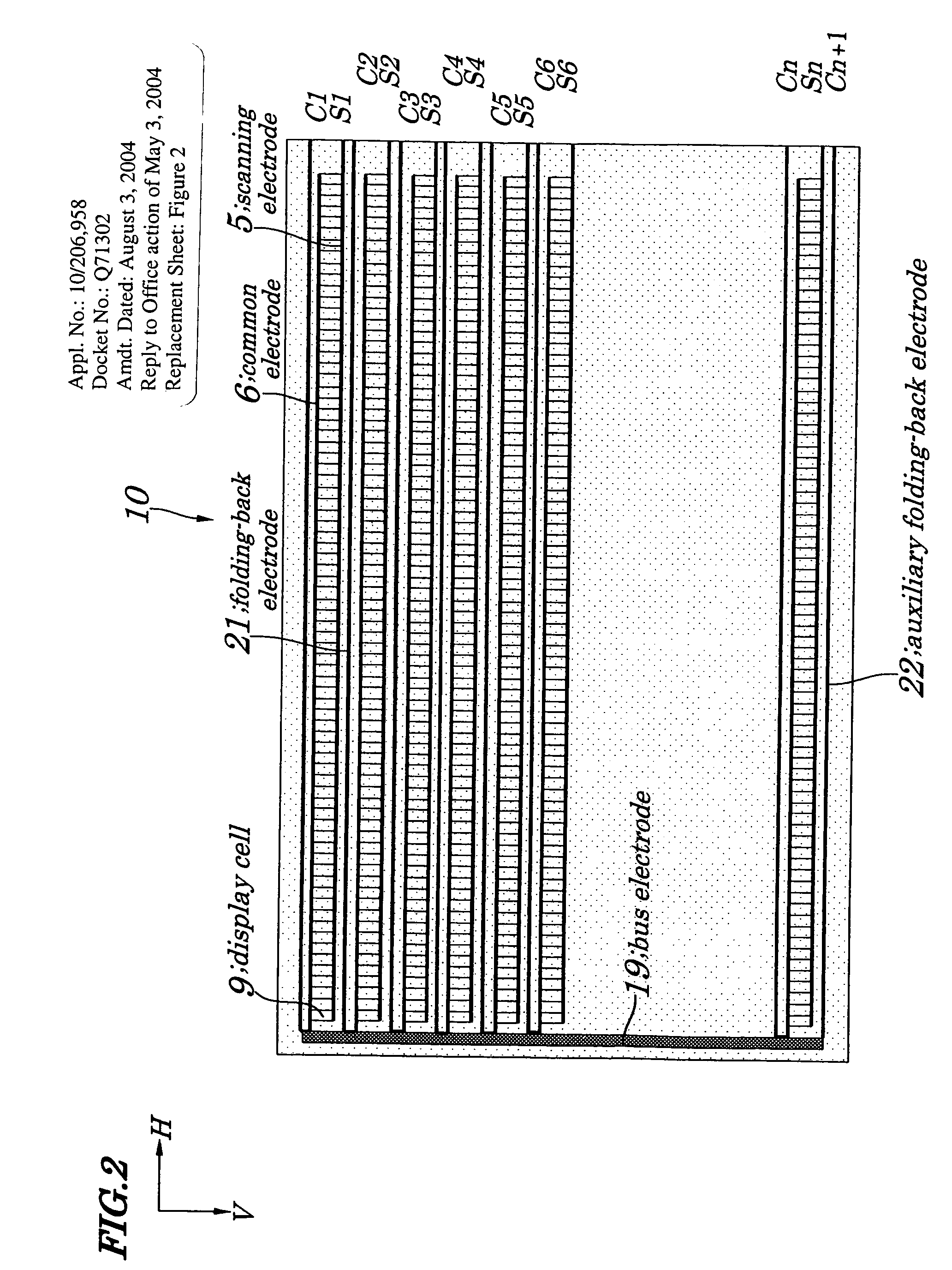
[0068]FIG. 4 is a plan view showing configurations of main components of a PDP device 20 of a second embodiment of the present invention. Configurations of the PDP device 20 of the second embodiment differ greatly from those in the first embodiment in that a folding-back electrode 21 is formed for alternating sequence of display rows. That is, in the PDP device 20 of the second embodiment, as shown in FIG. 4, a bus electrode 19 is connected to a common electrode 6 at a left end of a PDP panel which is used commonly by other common electrodes 6, and the folding-back electrode 21 to fold back the common electrode 6 to a right direction. At a right end of each of the folding-back electrodes 21 is formed each of driving terminals C1, C2, C3, . . . Cn. Moreover, at a right end of the scanning electrode 5 is formed each of the driving terminals S1, S2, S3, . . . Sn. In such the configurations, electrodes are arranged in a manner being symmetric with respect to the folding-back electrode 2...

third embodiment

[0077]FIG. 5 is a plan view showing configurations of main components of a PDP device 30 according to a third embodiment of the present invention. FIG. 6 is a schematic cross sectional view showing a method for driving the PDP device 30 according to the third embodiment. Configurations of the PDP device 30 of the third embodiment of the present invention differ greatly from configurations of the first embodiment in that each of the driving terminals of a scanning electrode 5 and a common electrode (sustaining electrode) is formed in a different direction for every one display row. That is, as shown in FIG. 5 and FIG. 6, in the PDP device 30 of the third embodiment, in the case when it is difficult to draw out each of driving terminals S1 to S2 and C1 and Cn of the scanning electrode 5 and a common electrode 6, respectively, from a same direction because of space constraints, these terminals are alternately formed at right end portions and left end portions for every one display row....


PUM


Abstract

A plasma display panel device is provided which is capable of obtaining a uniform state of light emission for displaying and of reducing electromagnetic radiation while easily achieving a high-definition image display. The plasma display panel device includes a pair of row electrodes made up of a scanning electrode and a common electrode (sustaining electrode) which provides one display row and formed in parallel with a face of a front substrate (scanning substrate) facing a rear substrate wherein a folding-back electrode is formed on a common electrode.

Description

BACKGROUND OF THE INVENTION[0001]1. Field of the Invention[0002]The present invention relates to a plasma display panel device and more particularly to a plasma display panel device having a pair of row electrodes made up of a scanning electrode and a common electrode (sustaining electrode) which provide one display row formed in parallel with a plane of a front substrate (scanning substrate) facing a rear substrate.[0003]The present application claims priority of Japanese Patent Application No. JP2001-230602 filed on Jul. 30, 2001, which is hereby incorporated by reference.[0004]2. Description of the Related Art[0005]A Plasma Display Panel device ((hereinafter, may be referred simply to as a PDP device) is classified into one of three types; one being an AC (Alternating Current)-type PDP device conventionally using an AC as a driving power source, another being a DC (Direct Current)-type PDP device using a DC as the driving power source, and a third being a hybrid-type PDP device u...

Claims


Application Information

Patent Timeline
Patent Type & Authority Patents(United States)
IPC IPC(8): G09G3/28H01J11/12H01J11/22H01J11/24H01J11/26H01J11/30H01J11/32H01J11/34H01J11/46
CPCG09G3/2986H01J11/22H01J11/28H01J11/12G09G2330/06H01J2211/28
Inventor SEKII, YOSHIZUMI
Owner PIONEER CORP
Why Eureka
Try Eureka