Liquid crystal display

a liquid crystal display and display technology, applied in non-linear optics, instruments, optics, etc., can solve the problems of reducing the aperture ratio and degrading the image quality, so as to reduce the load, improve the image quality, and reduce the light leakage

Inactive Publication Date: 2006-03-21
TCL CHINA STAR OPTOELECTRONICS TECH CO LTD
View PDF5 Cites 42 Cited by
  • Summary
  • Abstract
  • Description
  • Claims
  • Application Information

AI Technical Summary

Benefits of technology

[0006]Embodiments of the present invention decrease a load for a data wire to improve image qualities. Embodiments of the present invention decrease light leakage surrounding a data wire by decreasing a capacitance due to coupling between a data wire and a common electrode.

Problems solved by technology

In particular, a coupling of data lines and the common electrode drive the liquid crystal material therebetween to cause light leakage surrounding the data lines, thereby degrading image quality.
In addition, forming a black matrix widely in order to prevent light leakage tends to decrease the aperture ratio.

Method used


Image

  • Liquid crystal display
  • Liquid crystal display
  • Liquid crystal display

Examples


first embodiment

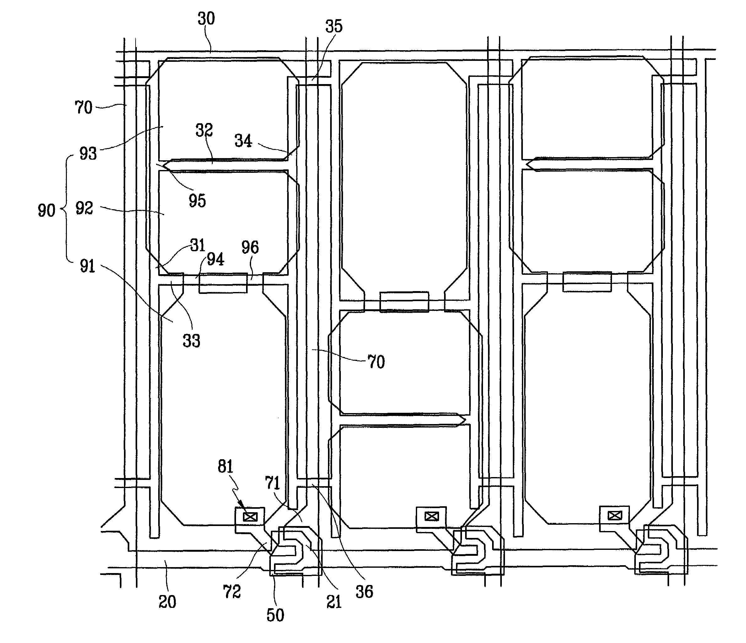
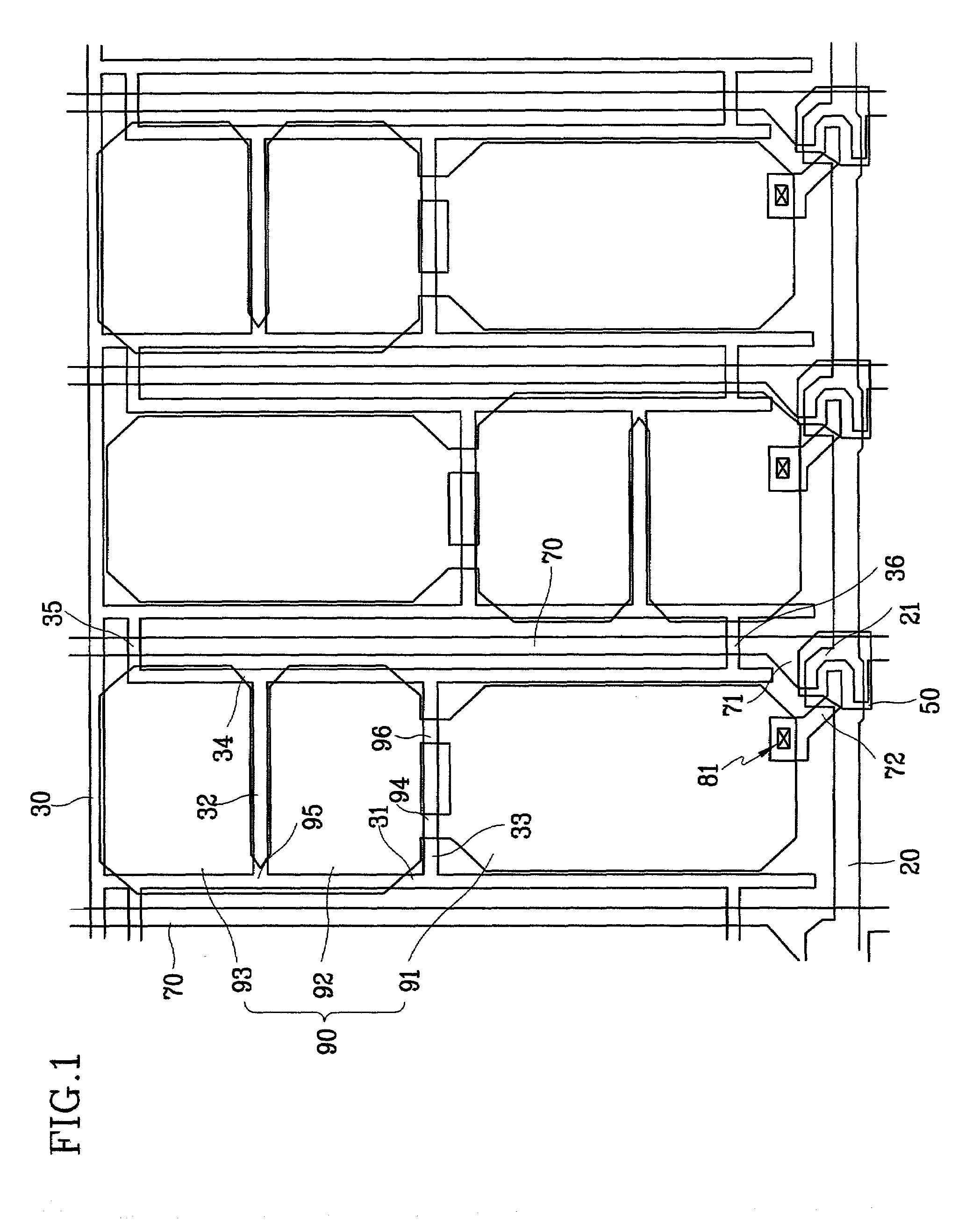
[0024]First, a thin film transistor of an LCD according to the present invention is described with reference to FIG. 1 and FIG. 4. A plurality of gate lines extending in a transverse direction formed on an insulating substrate 10, and the storage capacitor line 30 is formed parallel therewith. Several gate electrodes are formed as a projection shape on the gate lines and a first to a fourth storage electrode 31, 32, 33 and 34 and storage electrode connectors 35 and 36 on the storage capacitor line 30. Here, the first storage electrode 31 is directly connected to the storage capacitor line 30 to extend in a longitudinal direction, and each of the second and the third storage electrodes 32 and 33 are connected to the first storage electrode 31 to extend in a transverse direction. The fourth storage electrode 34 is connected to the second and the third storage electrodes 32 and 33 to extend in a longitudinal direction. The storage electrode connectors 35 and 36 connect the fourth stora...

second embodiment

[0036]In addition, since the data line apertures 440 belonging to the common electrode 400 overlap the data lines, the area of the common electrodes 400 overlapping the data lines is much decreased. As above, decreasing the area of the common electrode overlapping the data lines 70 enables loads of the data lines to decrease, and an amount of the variation of the liquid crystal capacitance in the data lines 70 to decrease, and side light leakage due to cross talk of data lines signals to decrease. In addition, since the light leakage surrounding the data lines is considerably decreased, the aperture ratio increases due to a decrease of the black matrix. The effect of disposing such data lines apertures 440 will be described more in detail after the present invention is described.

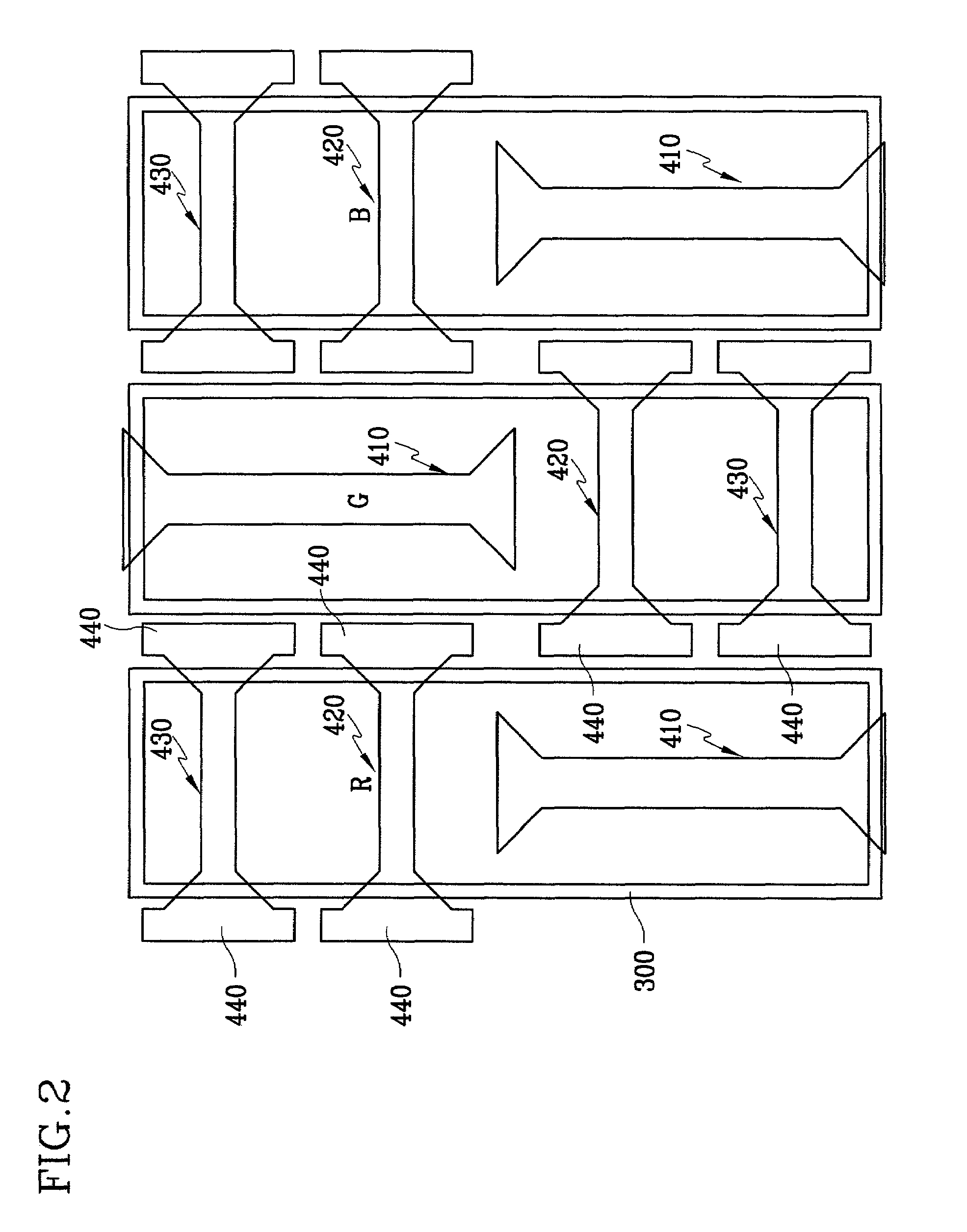
[0037]FIG. 5 is layout of pixel electrode apertures and common electrode apertures according to a second embodiment of the present invention when viewed from the front. The LCD according to the second embodi...

third embodiment

[0058]Another embodiment capable of obtaining the above effects will be described. FIG. 12 is a layout of pixel electrode and common electrode apertures when an LCD according to the present invention is seen at the front side.

[0059]As shown in FIG. 12, the structure of the LCD according to the third embodiment of the present invention is almost the same as that of the LCD and respective pixel areas according to the first embodiment of the present invention. However, it is different from the points that the pixel electrodes formed between the neighboring pixel areas are configured not to make 180 degree rotation symmetry but to repeat the same shape, and that the data line apertures 440 are disposed not on both sides of the second and the third apertures formed on the common electrode, but between the first aperture of the two neighboring pixel areas. The data line aperture 440 is disposed only between the first small parts 91 of the two neighboring pixel areas. The data line apertur...


PUM

PropertyMeasurementUnit
transmittanceaaaaaaaaaa
angleaaaaaaaaaa
dielectric constantaaaaaaaaaa

Abstract

A gate line and a data line are formed on a first panel, a pixel electrode is divided into several small parts by an aperture, and a thin film transistor is formed on a pixel area defined by the intersection thereof. A common electrode having a domain dividing aperture and a data line aperture is formed on a second panel disposed opposite to the first substrate. Removing the common electrode from an upper side of the data line by forming the data line aperture as above can result in decreasing load of the data line, reducing a variation amount of liquid crystal capacitance, decreasing light leakage of due to side cross talk, and increasing an aperture ratio.

Description

BACKGROUND OF THE INVENTION[0001](a) Field of the Invention[0002]The present invention relates to a liquid crystal display, and in particular, to a vertical alignment type of liquid crystal display to implement a wide viewing angle by dividing a pixel area into a plurality of small domains using a domain dividing means.[0003](b) Description of the Related Art[0004]Generally, a liquid crystal display (“LCD”) includes an upper panel where a common electrode and a color filter are formed and a lower panel where a thin film transistor and a plurality of pixel electrodes are formed with a liquid crystal material interposed therebetween. An LCD is a display device that displays desired images by applying electric fields to the liquid crystal layer to control the amount of light passing through the panels.[0005]A plurality of wires including a gate wire for transmitting scan signals and a data wire for transmitting image signals are formed on the thin film transistor panel, and these wires...

Claims


Application Information

Patent Timeline
Patent Type & Authority Patents(United States)
IPC IPC(8): G02F1/1343G02F1/1337G02F1/1333G02F1/1362
CPCG02F1/133707G02F1/134336G02F2001/134318G02F1/136213G02F1/134318G02F1/1337
Inventor SONG, JANG-KUN
Owner TCL CHINA STAR OPTOELECTRONICS TECH CO LTD
Why Eureka
Try Eureka