Semiconductor integrated circuit device

a technology of integrated circuits and semiconductors, applied in semiconductor devices, digital storage, instruments, etc., can solve the problems of source-drain resistance (parasitic resistance) components, differences in the low-level side margin of input signals, and significant decreases in low-level side margins of input signals. , to achieve the effect of suppressing relative deviation of operation characteristics, less occupation area, and well-stabilized operability

Inactive Publication Date: 2006-03-21
HITACHI LTD
View PDF6 Cites 195 Cited by
  • Summary
  • Abstract
  • Description
  • Claims
  • Application Information

AI Technical Summary

Benefits of technology

[0009]It is possible to lessen the occupation area of CMOS circuitry having rectangular gates. It is also possible to suppress relative deviation of operation characteristics of a plurality of CMOS circuits. It becomes possible for the CMOS circuits to offer well-stabilized operability.

Problems solved by technology

Accordingly, when designing the CMOS configuration at the same size, its logic threshold is shifted or “offset” to its low level side, resulting in a significant decrease in low-level side margin of an input signal.
Nevertheless, the above-noted patent documents lack any teachings as to this point.
Furthermore, in the process of consideration of circuit layout designs in the case of using MOSFETs with ring-shaped gates, it has been found that the layout of source / drain contacts and gate draw-out portions results in differences in source-drain resistance (parasitic resistance) components, which in turn causes the MOSFETs to vary or deviate in operation characteristics.

Method used


Image

  • Semiconductor integrated circuit device
  • Semiconductor integrated circuit device
  • Semiconductor integrated circuit device

Examples


Embodiment Construction

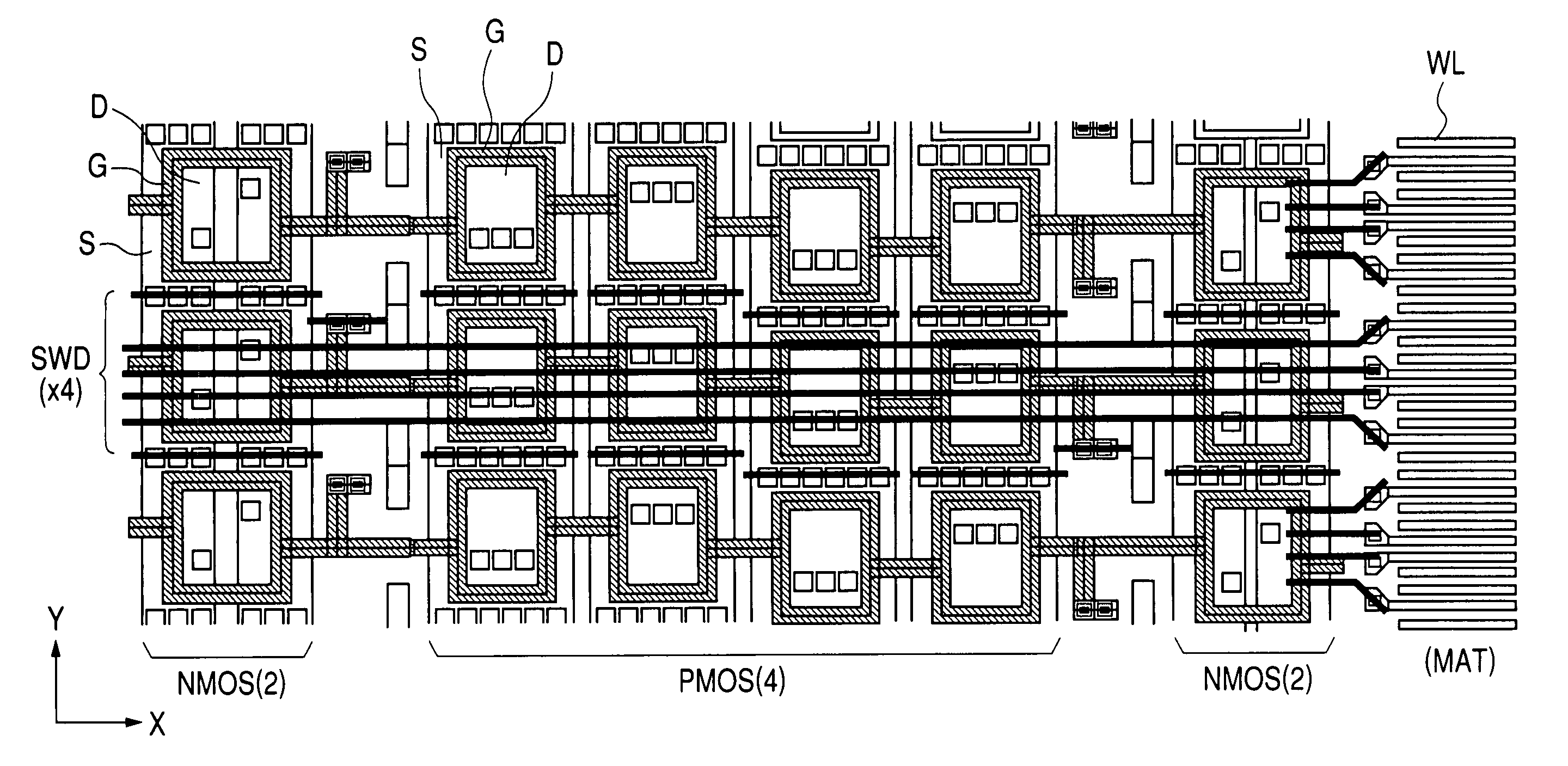
[0025]Referring to FIG. 1, there is shown a layout diagram of one embodiment of a sub-word driver unit in accordance with this invention. In this embodiment, MOSFETs making up four sub-word drivers corresponding to four sub-word lines WL are formed so that these are arrayed in a word-line direction (X direction in FIG. 1). The subword drivers SWD are such that each is operable to drive subword lines WL which are provided in two memory mats (sub-arrays) that are formed to put it therebetween, as will be described later. There are exemplarily shown in FIG. 1 those subwordlines WL that are provided in one of the two memory mats, which is located on one end side in the X direction.

[0026]In a chip surface area in which the above-noted four subword drivers SWD (x4) are formed, a total of eight subwordlines WL are allocated. Since a respective one of the subword drivers is the one that drives the subwordlines WL of two memory mats that interpose it therebetween as stated previously, when l...


PUM


Abstract

A semiconductor integrated circuit device capable of achieving higher integration and simplification of manufacturing processes is provided. Circuitry is provided which includes a first N-channel MOSFET and a first p-channel MOSFET each having a gate insulating dielectric film with a first film thickness, wherein a poly-silicon layer making up a gate electrode is doped with an N-type impurity. The circuitry also includes a second N-channel MOSFET having a gate insulator film with a second film thickness thinner than the first thickness, wherein an N-type impurity is doped into a polysilicon layer making up a gate electrode, and a second P-channel MOSFET with a P-type impurity being doped into a polysilicon layer making up a gate electrode. The gate electrodes of the first N-channel MOSFET and first P-channel MOSFET are integrally formed and mutually connected together.

Description

INCORPORATION BY REFERENCE[0001]The present application claims priority from Japanese application JP2003-346500 filed on Oct. 6, 2003, the content of which is hereby incorporated by reference into this application.[0002]1. Field of the Invention[0003]The present invention relates to semiconductor integrated circuit devices and also relates to effective techniques for use with element layout architectures of sub-word drivers of hierarchical word-line schemes of dynamic random access memories (DRAMs) by way of example.BACKGROUND OF THE INVENTION[0004]An example of DRAMs capable of shrinking the area of word-line driver circuitry by use of P-channel MOSFETs of the so-called ring type is disclosed in U.S. Pat. No. 6,236,258B1. In addition, an example that employs ring-shaped gate electrodes to accomplish breakdown voltage enhancement is found in JP-A-10-050957.[0005]In the devices as taught by the above-identified Japanese patent documents, each is such that the ring-shaped gate MOSFETs...

Claims


Application Information

Patent Timeline
Patent Type & Authority Patents(United States)
IPC IPC(8): G11C5/06G11C11/401G11C11/408G11C11/4097H01L21/8238H01L21/8242H01L27/02H01L27/092H01L27/105H01L27/108
CPCG11C11/4087G11C11/4097H01L27/0922H01L27/105H01L27/0207H01L27/10894H10B12/09
Inventor KAWAMATA, TSUNEOHASEGAWA, MASATOSHITORIYAMA, KEINOSUKEHOKARI, TOMOFUMI
Owner HITACHI LTD
Why Eureka
Try Eureka