Semiconductor device analyzer, method for analyzing/manufacturing semiconductor device, and storage medium storing program for analyzing semiconductor device

a semiconductor device and analyzer technology, applied in error detection/correction, computation using non-denominational number representation, instruments, etc., can solve the problems of time and money, waste time and money, trouble will arise during the manufacturing of semiconductor devices, etc., to achieve efficient analysis of parasitic elements and without increasing operational scale

Inactive Publication Date: 2006-03-21
KK TOSHIBA
View PDF5 Cites 22 Cited by
  • Summary
  • Abstract
  • Description
  • Claims
  • Application Information

AI Technical Summary

Benefits of technology

[0018]An object of the present invention is to provide a semiconductor device analyzer capable of efficiently analyzing the influence of parasitic elements in a semiconductor substrate without increasing operational scale.
[0019]Another object of the present invention is to provide a method for analyzing a semiconductor device with use of a substrate network model of three-dimensional meshes involving not only resistive elements but also capacitive elements. This method is capable of efficiently and correctly analyzing the influence of parasitic elements in a semiconductor device.
[0020]Still another object of the present invention is to provide a computer program encompassing a storage medium and a program recorded on the storage medium, the a program efficiently analyzes the influence of parasitic elements in a semiconductor substrate without increasing computation processes.

Problems solved by technology

Testing and evaluating these complicated and advanced semiconductor devices need time and money if they must actually be fabricated for each test or evaluation.
The semiconductor devices with high-frequency analog circuits, analog-digital mixed circuits, and high-speed digital circuits involve a problem that signals transmitting through a semiconductor substrate interfere with circuit elements merged in the substrate.
Analyzing a semiconductor device involves errors, and if the errors are large, trouble will arise during the manufacturing of the semiconductor device.
If the prototype semiconductor device shows unacceptable behaviors, it must be redesigned and reproduced through the long and intricate processes, to waste time and money.
There is no way to restore time loss caused by design failure.
Semiconductor industries are competing for higher-performance semiconductor devices, and the most critical issue for them is a development speed.
If finer meshes are defined to improve the correctness of the resistive network, even the substrate part of a given semiconductor device will involve a large-scale network to take a simulation time longer than an actual fabrication time, or in some case, the analysis itself will fail.
This technique, however, is not practical.
Programming the symbolical processes, however, is practically impossible because original equations to be reduced are of large scale and are complicated with several thousands of variables.
This results in elongating an analysis time and impeding analysis.
The earlier methodology, therefore, is unable to correctly analyze the influence of parasitic elements in the semiconductor substrate nor efficiently design the semiconductor device.
The conventional Y-matrix reduction technique of eliminating irrelevant nodes is impractical.

Method used


Image

  • Semiconductor device analyzer, method for analyzing/manufacturing semiconductor device, and storage medium storing program for analyzing semiconductor device
  • Semiconductor device analyzer, method for analyzing/manufacturing semiconductor device, and storage medium storing program for analyzing semiconductor device
  • Semiconductor device analyzer, method for analyzing/manufacturing semiconductor device, and storage medium storing program for analyzing semiconductor device

Examples


Embodiment Construction

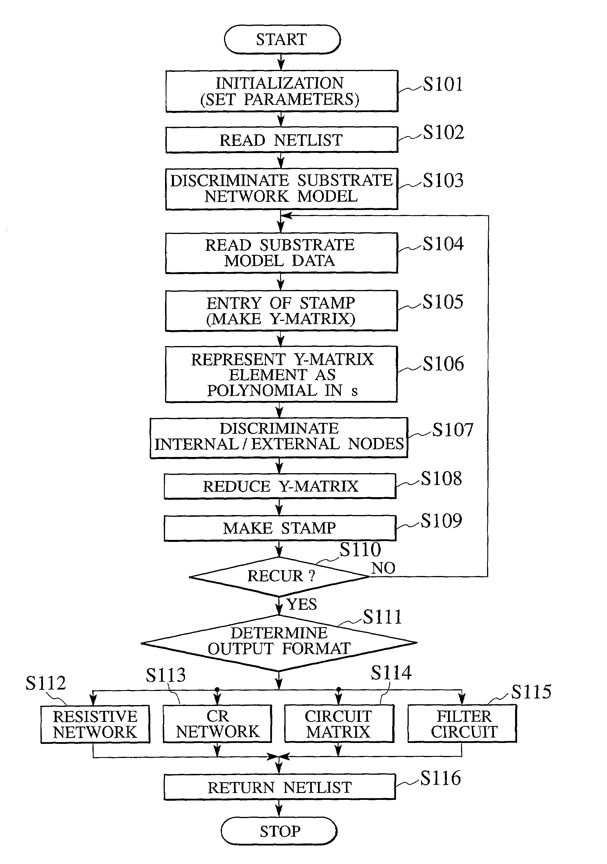
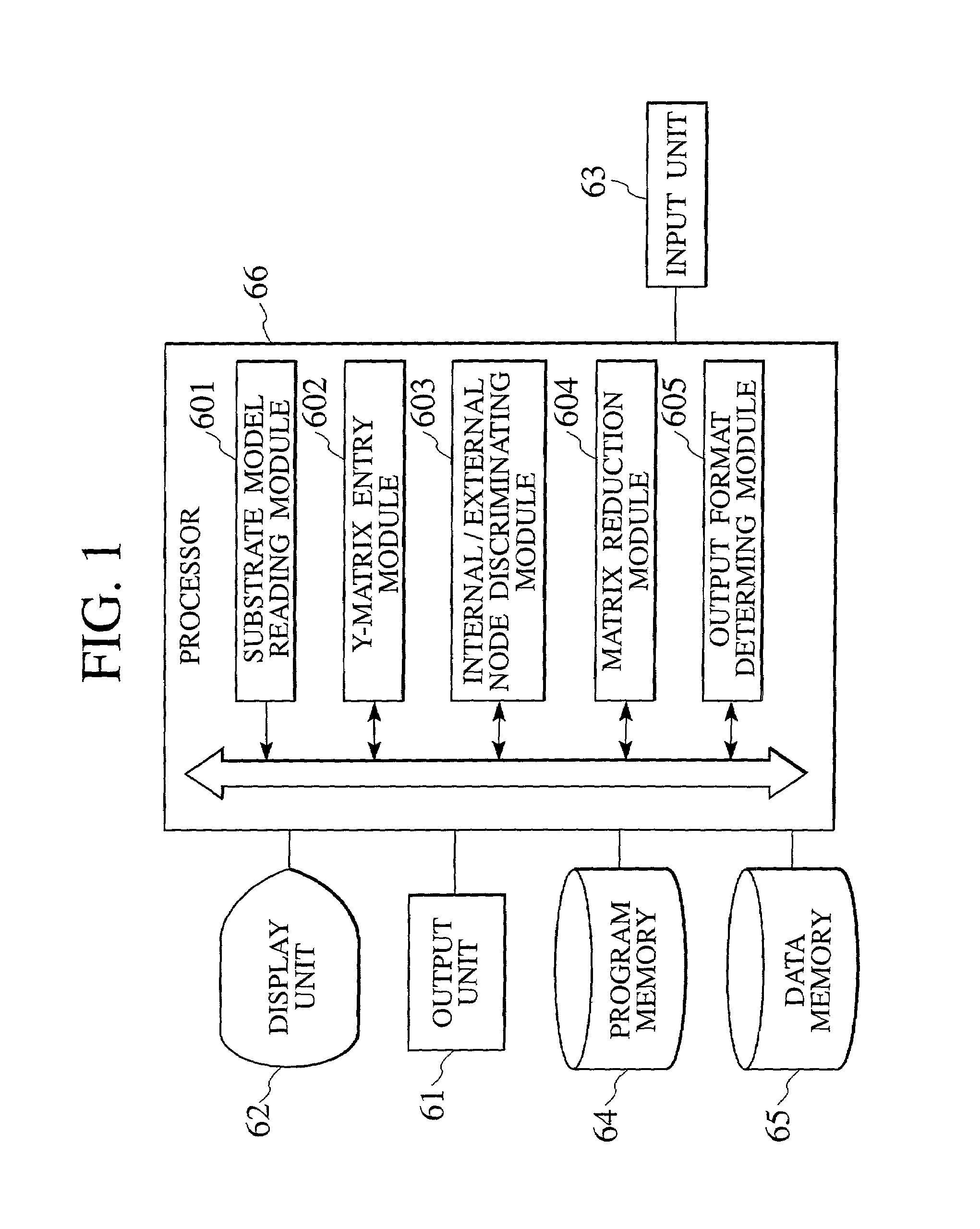
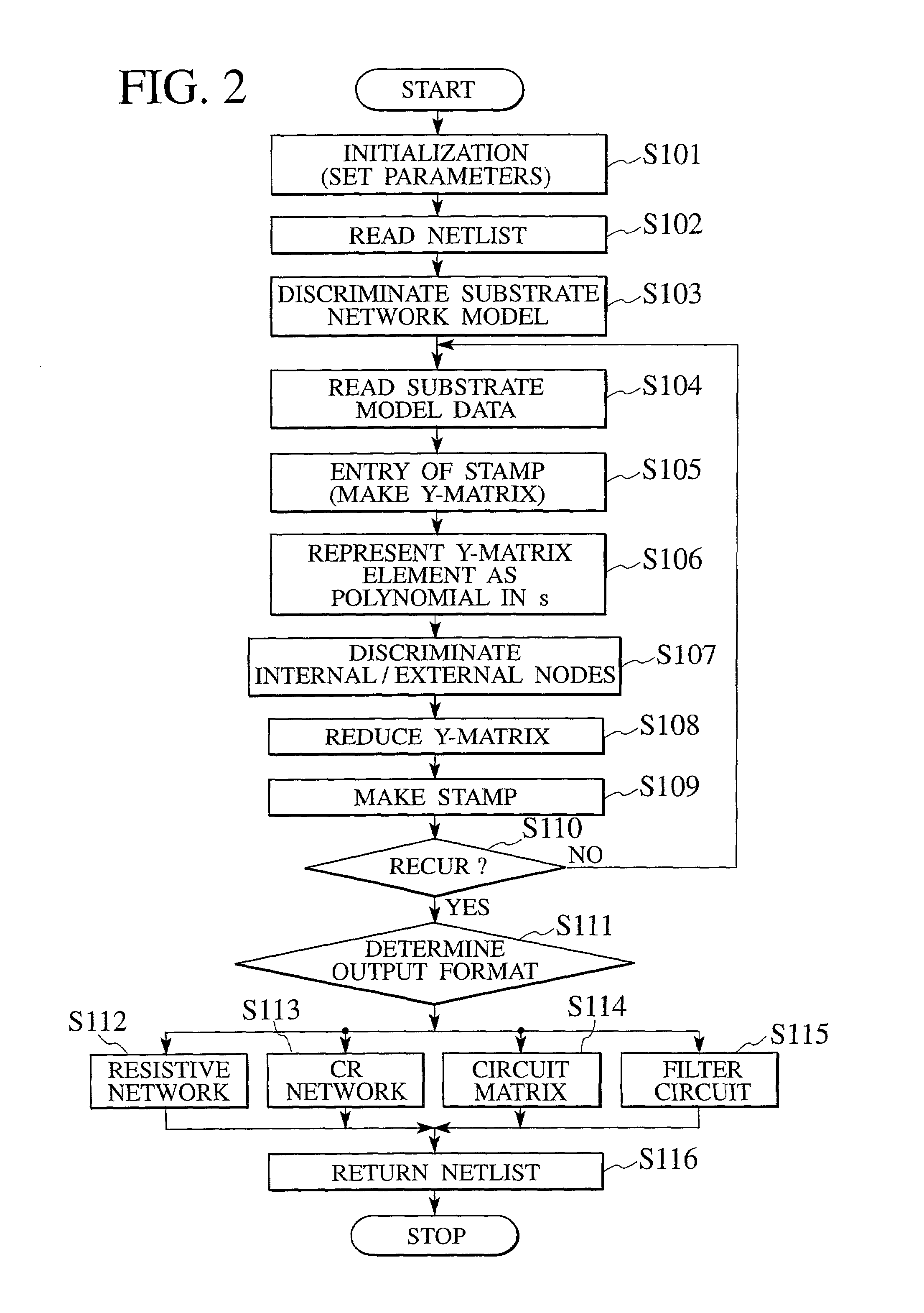
[0061]Various embodiments of the present invention will be described with reference to the accompanying drawings. It is to be noted that the same or similar reference numerals are applied to the same or similar parts and elements throughout the drawings, and the description of the same or similar parts and elements will be omitted or simplified. Generally and as it is conventional in the representation of semiconductor devices, it will be appreciated that the various drawings are not drawn to scale from one figure to another nor inside a given figure, and in particular, that the layer thicknesses are arbitrarily drawn for facilitating the reading of the drawings. In the following descriptions, numerous specific details are set forth such as specific signal values, etc., to provide a thorough understanding of the present invention. However, it will be obvious to those skilled in the art that the present invention may be practiced without such specific details. In other instances, wel...


PUM


Abstract

A semiconductor device analyzer has a substrate model reading module, a Y-matrix entry module, a discriminating module, a matrix reduction module, and an output format discriminating module. The substrate model reading module reads a substrate network model of three-dimensional meshes representing the substrate of a semiconductor device. The substrate network model is a network of resistive and capacitive elements and is used for the simulation and analysis of the semiconductor substrate. The Y-matrix entry module prepares a Y-matrix from the substrate network model, each element of the Y-matrix being expressed with a polynomial of differential operator “s”. The discriminating module discriminates internal nodes to be eliminated from external nodes to be left among the nodes of the substrate network model. The matrix reduction module eliminates the internal nodes, thereby reducing the Y-matrix. The output format determining module determines an output format for an operation result.

Description

BACKGROUND OF THE INVENTION[0001]1. Field of the Invention[0002]The present invention pertains to a method for manufacturing a semiconductor device, a method for efficiently simulating and analyzing the structure of a semiconductor device during a device designing stage, a semiconductor device analyzer for carrying out such a method, and a storage medium storing a program to execute such a method. In particular, the present invention relates to a method for efficiently analyzing the influence of parasitic elements embraced in a semiconductor substrate on which fine circuit patterns are formed, an analyzer for executing such a method, and a storage medium storing a program to execute such a method.[0003]2. Description of the Related Art[0004]Semiconductor devices with high-frequency analog circuits, analog-digital mixed circuits, and high-speed digital circuits have fine circuit patterns delineated by, for example, photolithography on semiconductor substrates made of, for example, si...

Claims


Application Information

Patent Timeline
Patent Type & Authority Patents(United States)
IPC IPC(8): G06F17/10G06F17/50G01R31/316H01L21/82
CPCG06F17/5036G06F30/367
Inventor KIMURA, TOMOHISAOKUMURA, MAKIKO
Owner KK TOSHIBA
Why Eureka
Try Eureka