Pull-back method of forming fins in FinFets

a technology of finfets and fins, which is applied in the direction of transistors, semiconductor devices, electrical apparatus, etc., can solve the problems of degrading the ability of the gate to control whether the device is placed or not, affecting the operation of the gate, and increasing the difficulty of mosfets

Inactive Publication Date: 2006-03-28
INT BUSINESS MASCH CORP
View PDF3 Cites 83 Cited by
  • Summary
  • Abstract
  • Description
  • Claims
  • Application Information

AI Technical Summary

Problems solved by technology

As MOSFETs are scaled to channel lengths below 100 nm, conventional MOSFETs suffer from several problems.
In particular, interactions between the source and drain of the MOSFET degrade the ability of the gate to control whether the device is on or off.
As device size is scaled, however, this becomes increasingly difficult, since the distance between the source and drain is reduced, and hence, they increasingly interact with the channel, reducing gate control and increasing short channel effects (SCE).
As the dimensions of structures or features on the integrated circuit reach levels below 100 nm or 50 nm, lithographic techniques are unable to precisely and accurately define the feature.
However, patterning narrow, dense active regions is challenging.
As discussed above with respect to gate conductors, conventional lithographic tools are unable to accurately and precisely define active regions as structures or features with dimensions below 100 nm or 50 nm.

Method used


Image

  • Pull-back method of forming fins in FinFets
  • Pull-back method of forming fins in FinFets
  • Pull-back method of forming fins in FinFets

Examples


Embodiment Construction

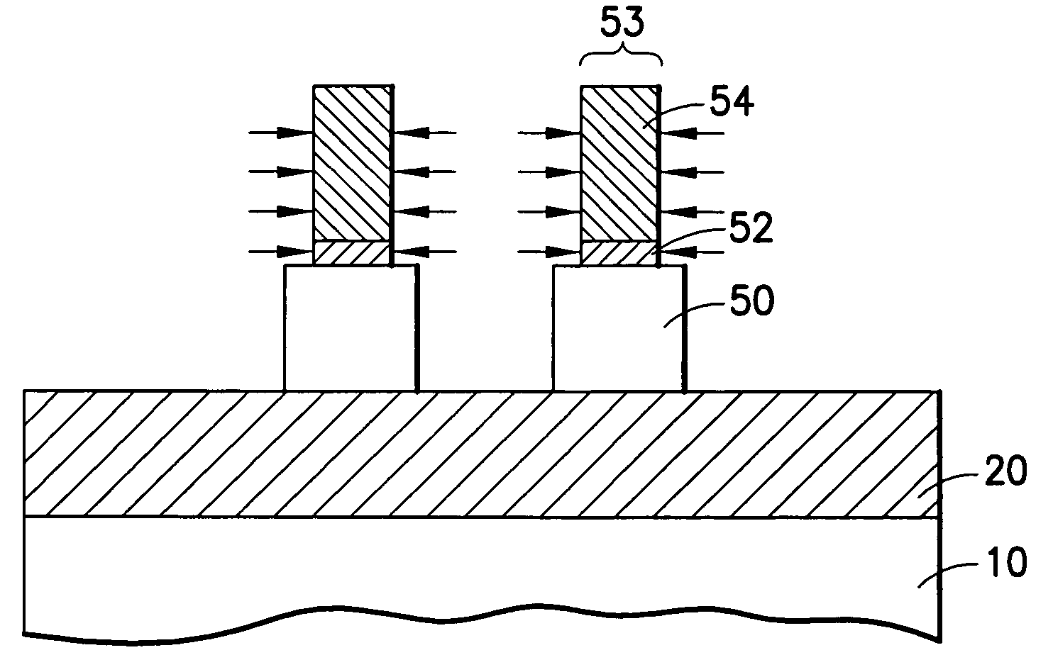
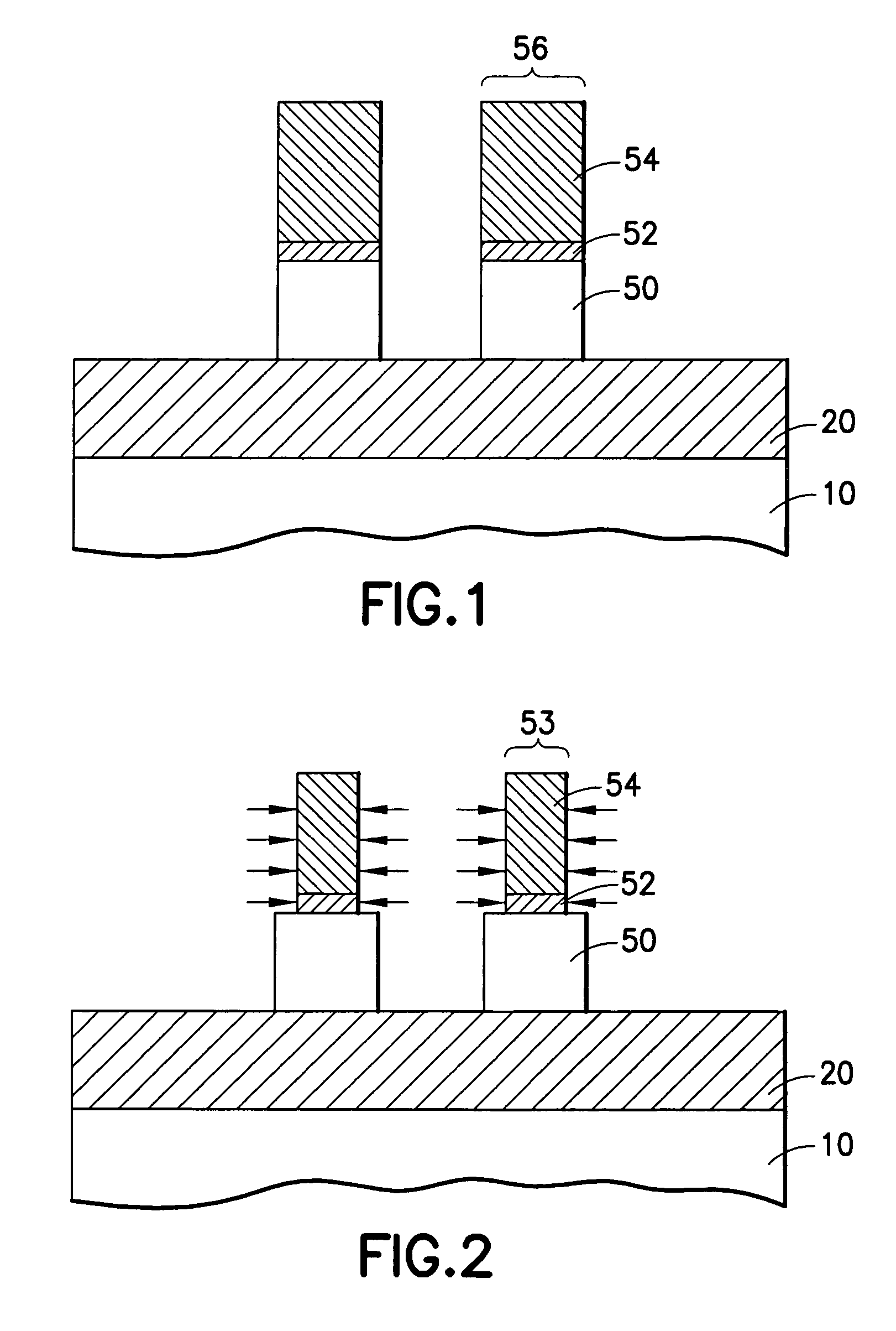
[0036]This invention describes a process for forming controlled, thin body fins for a FinFET device, in which the uniformity of the thickness of the fins does not depend on alignment of a stepper. The process uses a pullback step that defines the width of the hardmask that sets the thickness of the fin. Thickness control of the fin body is a critical factor in the fabrication process, as it directly results in FET threshold variation.

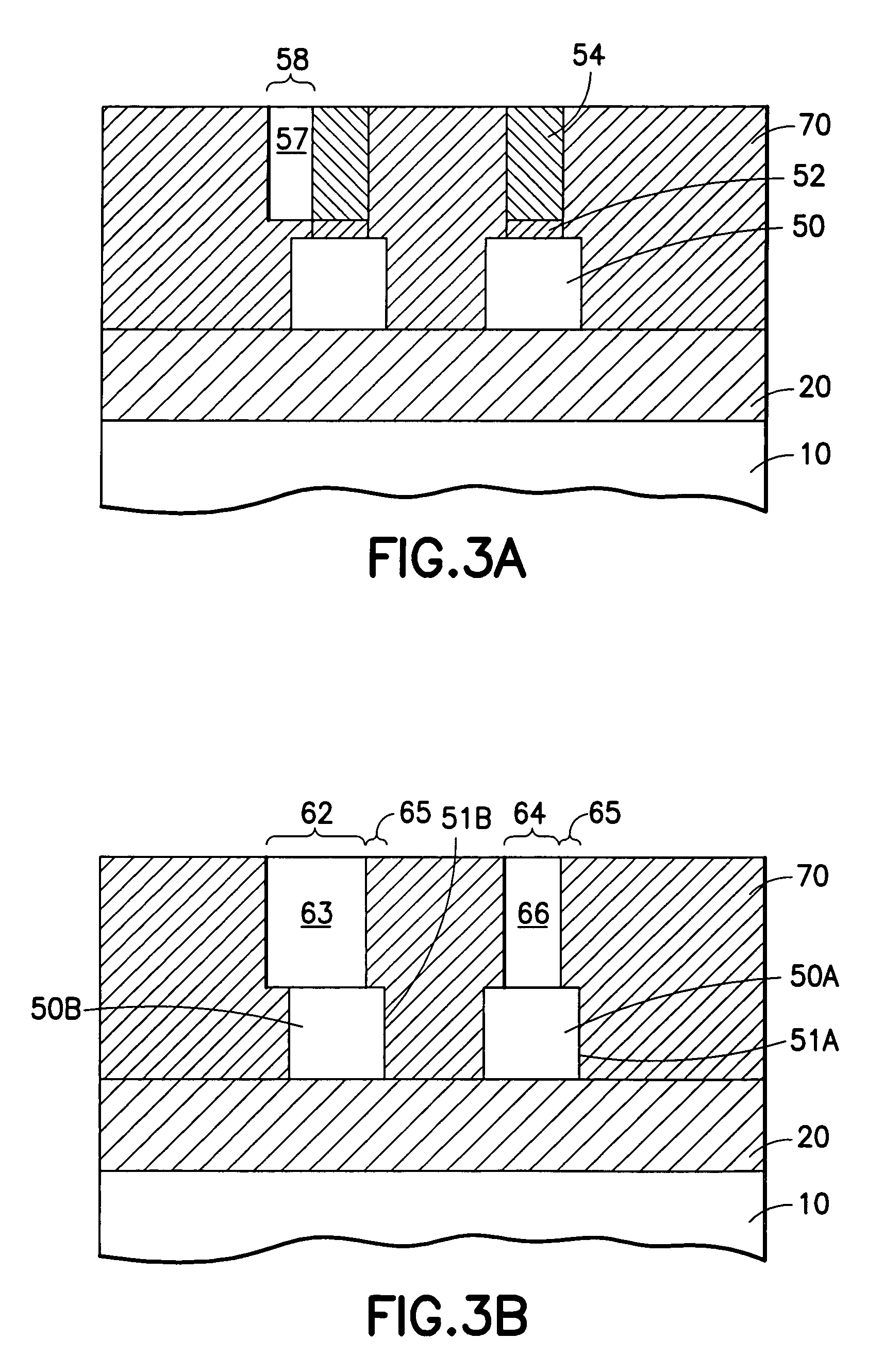
[0037]This specification describes two integration schemes of the pullback fin process, the first scheme is implemented in a self-aligned source / drain process flow and the second in a source / drain block process flow.

[0038]In each case, the starting point is a SOI or bulk silicon wafer. In the case of a SOI wafer, the fin height will be determined by the thickness of the silicon. The layer of semiconductor that contains the fins will be referred to as the fin layer, whether the substrate is bulk or SOI.

[0039]Referring now to FIG. 1, there is shown in cro...


PUM


Abstract

A method of forming integrated circuits having FinFET transistors includes a method of forming sub-lithographic fins, in which a mask defining a block of silicon including a pair of fins in reduced in width or pulled back by the thickness of one fin on each side, after which a second mask is formed around the first mask, so that after the first mask is removed, an aperture remains in the second mask having the width of the separation distance between the pair of fins. When the silicon is etched through the aperture, the fins are protected by the second mask, thereby defining fin thickness by the pullback step. An alternative method uses lithography of opposite polarity, first defining the central etch aperture between the two fins lithographically, then expanding the width of the aperture by a pullback step, so that filling the widened aperture with an etch-resistant plug defines the outer edges of the pair of fins, thereby setting the fin width without an alignment kstep.

Description

TECHNICAL FIELD[0001]The field of the invention is that of fabricating field effect transistors having a body extending perpendicular to the semiconductor substrate between horizontally disposed source and drain regions, referred to as a “FinFET”.BACKGROUND OF THE INVENTION[0002]Metal-Oxide-Semiconductor field effect transistor (MOSFET) technology is the dominant electronic device technology in use today. Performance enhancement between generations of devices is generally achieved by reducing the size of the device, resulting in an enhancement in device speed. This is generally referred to as device “scaling”.[0003]Ultra-large-scale integrated (ULSI) circuits generally include a multitude of transistors, such as more than one million transistors and even several million transistors that cooperate to perform various functions for an electronic component. The transistors are generally complementary metal oxide semiconductor field effect transistors (CMOSFETs) which include a gate cond...

Claims


Application Information

Patent Timeline
Patent Type & Authority Patents(United States)
IPC IPC(8): B44C1/22H01L21/308H01L21/336H01L29/78H01L29/786
CPCH01L21/3086H01L29/785H01L29/66795H01L21/3088
Inventor BEINTNER, JOCHEN C.CHIDAMBARRAO, DURESETILI, YUJUNSETTLEMYER, JR., KENNETH T.
Owner INT BUSINESS MASCH CORP
Why Eureka
Try Eureka